Eureka AIR delivers breakthrough ideas for toughest innovation challenges, trusted by R&D personnel around the world.

Semiconductor layer material-indium zinc titanium oxide for oxide thin film transistor

A thin-film transistor and oxide thin-film technology, which is applied in the field of oxide materials, can solve problems such as high cost, can only be used as switching elements, and poor device stability.

Inactive Publication Date: 2011-08-24
FUDAN UNIV
View PDF1 Cites 6 Cited by
  • Summary
  • Abstract
  • Description
  • Claims
  • Application Information

AI Technical Summary

Problems solved by technology

This type of TFT uses α-Si film as the semiconductor layer, which can be prepared on a large-area glass substrate by traditional film deposition process, so the cost is low, but its field-induced mobility is generally less than 1 cm 2 / V s, and the stability of the device is poor under the action of voltage pressure, usually it can only be used as a switching element
The poly-Si TFT with polysilicon (poly-Si) as the semiconductor layer has a field-induced mobility 1-2 orders of magnitude higher than that of the α-Si TFT, and is also superior in device stability. It can not only be used as a switching element, It can also be used as a driving element to form an auxiliary driving circuit, but the preparation process is complicated, the cost is high, and it is difficult to apply to large-area substrates

Method used


Image

  • Semiconductor layer material-indium zinc titanium oxide for oxide thin film transistor
  • Semiconductor layer material-indium zinc titanium oxide for oxide thin film transistor
  • Semiconductor layer material-indium zinc titanium oxide for oxide thin film transistor

Examples


Embodiment Construction

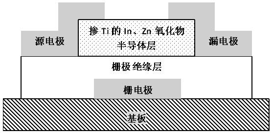
[0017] Examples of Ti-doped In, Zn oxides and TFTs based on such semiconductor materials according to the present invention will be given below.

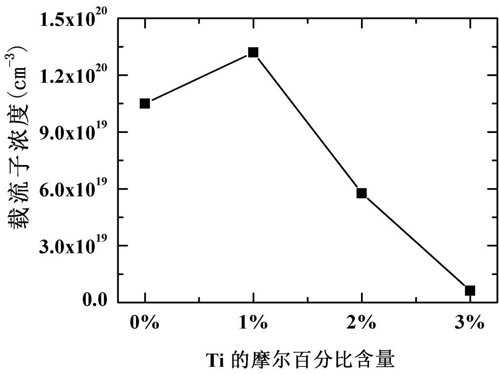
[0018] figure 1 shows the effect of Ti content on In 2 Zn 2 o 5 Effect of thin film carrier concentration. Doped with Ti In 2 Zn 2 o 5 The films were prepared under the same process conditions using targets with different amounts of Ti doped, and the substrate temperature was 170 °C during film deposition. The mole percentage content of Ti in the figure refers to the mole percentage of Ti relative to the total amount of In, Zn and Ti. At low Ti content, Ti may act as a donor, replacing In or Zn with 1 to 2 electrons to increase the carrier concentration. When the content of Ti in the film increased to 1%, its effect of reducing the carrier concentration began to appear. In order to achieve the purpose of reducing the carrier concentration, a sufficiently high Ti content is required, and the specific value needs to be determ...


PUM


Abstract

The invention belongs to the technical field of thin film transistor devices, in particular relating to a semiconductor layer material for an oxide thin film transistor. The semiconductor layer material is an indium zinc titanium oxide, wherein the proportion of components, namely indium, zinc and titanium is controlled within a certain range. The invention further provides a thin film transistor using the oxide as a trench layer material. The obtained thin film transistor has good application prospects in the field of flat panel display.

Description

technical field [0001] The invention belongs to the technical field of thin film transistors, and in particular relates to an oxide material that can be used for a semiconductor layer of a thin film transistor. Background technique [0002] Thin Film Transistor (TFT) is a general term for field effect transistors whose semiconductor layer is a thin film structure. TFT is used as an auxiliary component in various display or sensing devices, especially in liquid crystal displays (Liquid Crystal Displays, LCD), which provides a technical basis for LCD to achieve higher image quality and large area. For new displays such as Organic Light Emitting Displays (Organic Light Emitting Displays, OLED) and electronic paper, the use of TFT technology can also effectively improve performance. [0003] At present, the most widely used in LCD is amorphous silicon (α-Si) TFT. This type of TFT uses α-Si film as the semiconductor layer, which can be prepared on a large-area glass substrate b...

Claims


Application Information

Patent Timeline
IPC IPC(8): H01L29/786H01L29/26
Inventor 姚绮君李曙新张群
Owner FUDAN UNIV
Why Eureka
Eureka Blog
Learn More