PNP bipolar transistor in SiGe BiCMOS technology

A bipolar transistor and process technology, used in semiconductor devices, semiconductor/solid-state device manufacturing, electrical components, etc., can solve the problems of long base region width, difficult to reduce the area, difficult to improve the PNP current amplification factor, etc., to achieve the current amplification factor The effect of increasing and reducing the area

Active Publication Date: 2011-06-08
SHANGHAI HUAHONG GRACE SEMICON MFG CORP
View PDF0 Cites 15 Cited by
  • Summary
  • Abstract
  • Description
  • Claims
  • Application Information

AI Technical Summary

Problems solved by technology

like figure 1 As shown, it is a schematic diagram of the device structure of the existing PNP, which is a lateral structure and includes three active regions, which are in turn from left to right: base lead-out region (N-type Sinker), collector region and emitter region, which is It is determined that its area is difficult to shrink; its emitter region is a P-type epitaxial layer, and the base region is located under the P-type epitaxial layer, and pass...

Method used


Image

  • PNP bipolar transistor in SiGe BiCMOS technology
  • PNP bipolar transistor in SiGe BiCMOS technology
  • PNP bipolar transistor in SiGe BiCMOS technology

Examples


Embodiment Construction

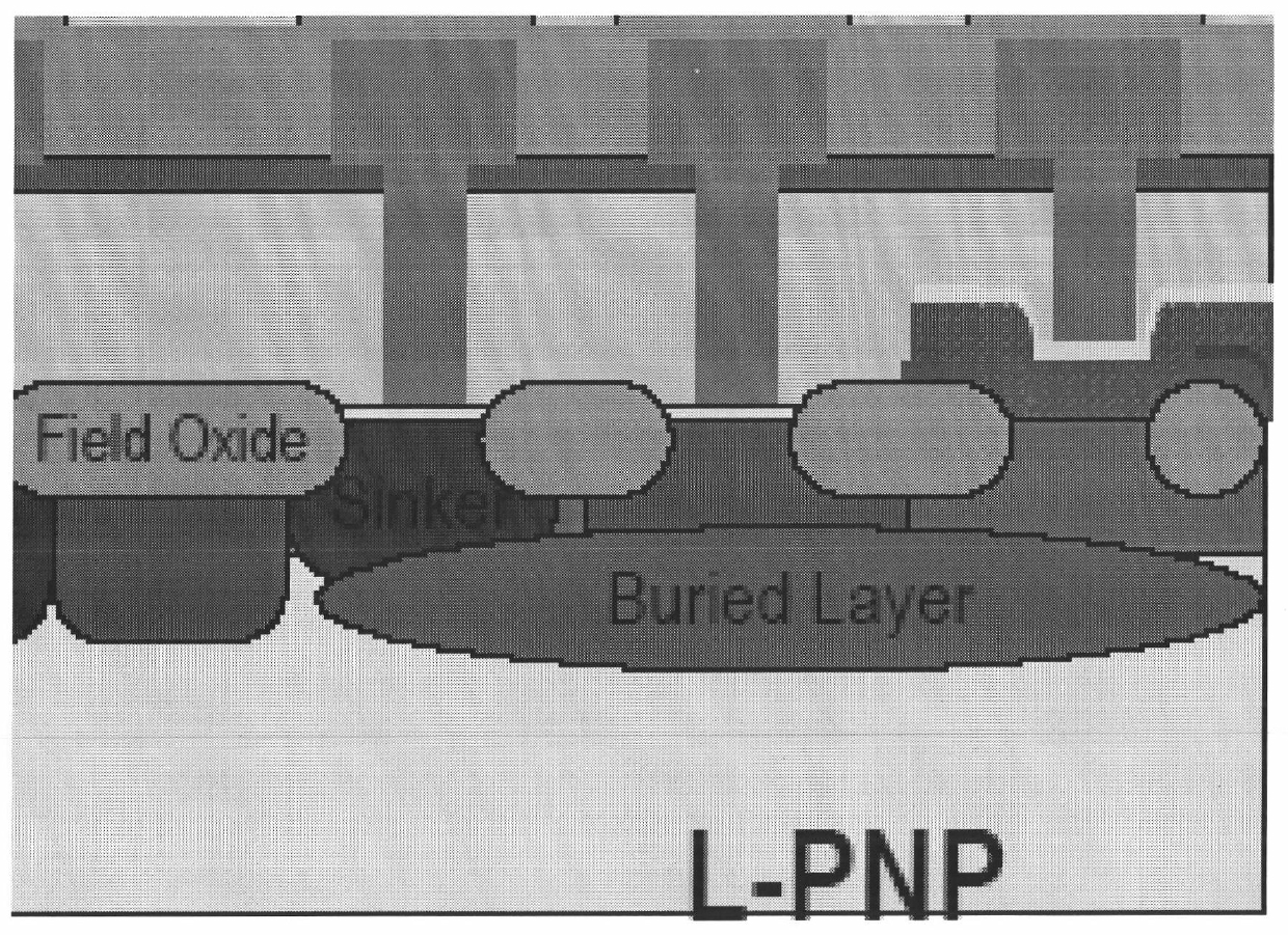
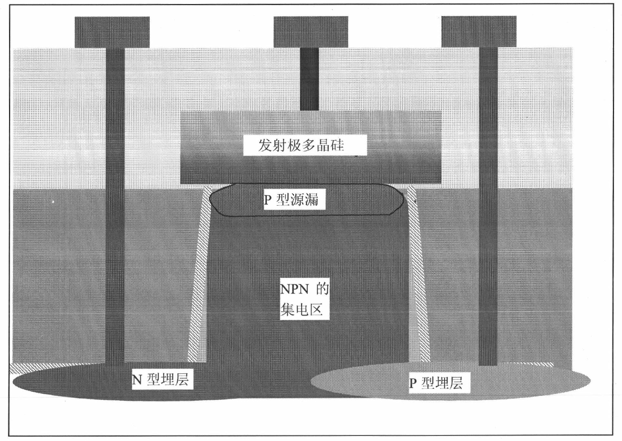
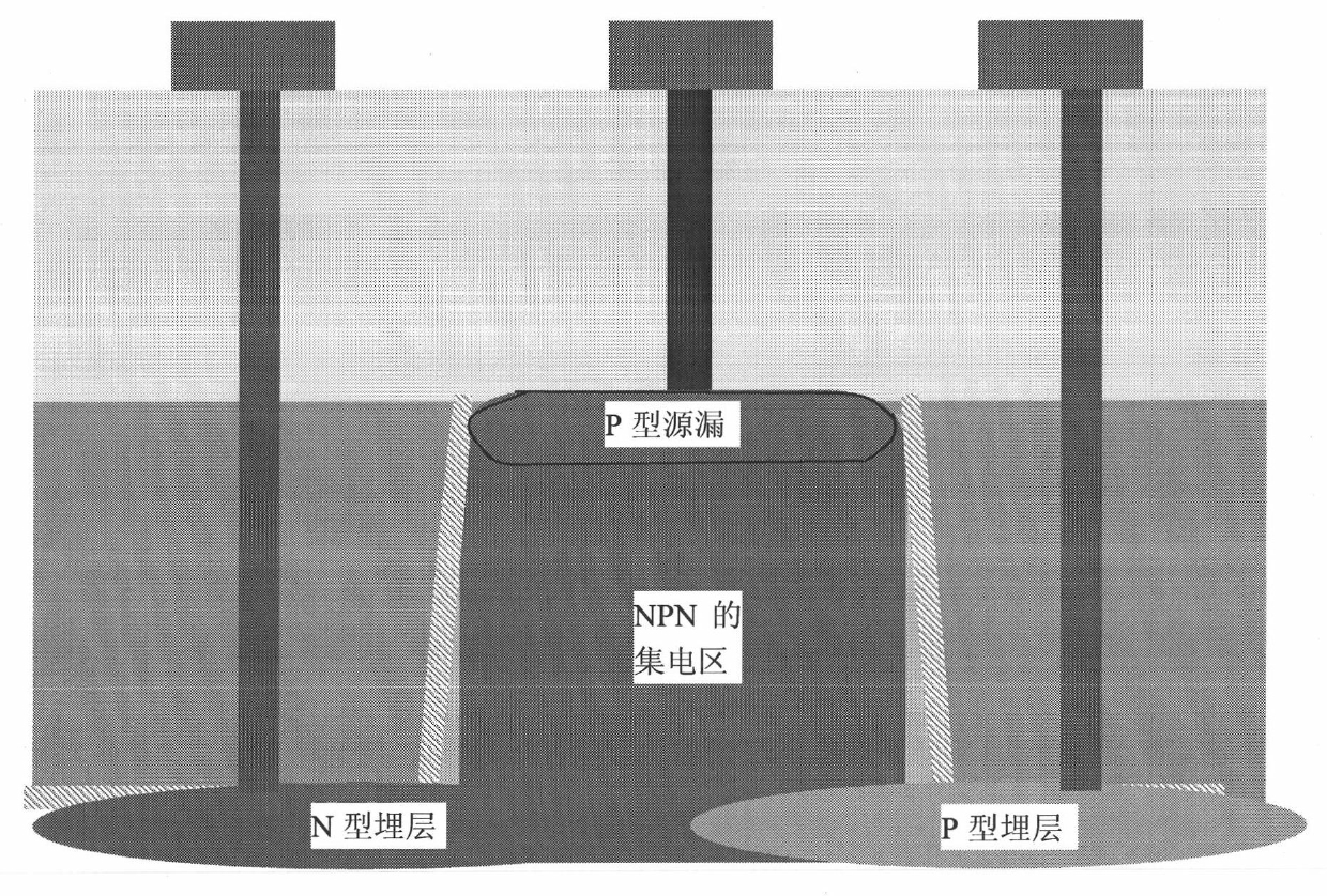
[0016] Such as Figure 2A with Figure 2B Shown is a schematic diagram of the structure of a PNP bipolar transistor in the SiGe BiCMOS process of the present invention. The active region is isolated by a shallow trench field oxide layer, including:

[0017] A collector region is formed by a P-type buried layer located at the bottom of the shallow trench, and the collector region is drawn by forming a deep well contact on the field oxide layer. The P-type buried layer is formed by ion implantation after the shallow trench is formed and before the field oxide layer is filled. The hard mask layer on the active area is locally self-aligned and implanted to ensure that there is no active area. Impurities implanted by the P-type buried layer; B or BF selectively implanted by the P-type buried layer 2 , The injection dose is 1e12~1e14cm -2 , The implant energy is subject to not penetrating the hard mask layer.

[0018] A base area, as Figure 2A with Figure 2B The collector region of the...


PUM


Abstract

The present invention discloses a PNP bipolar transistor in a SiGe BiCMOS (Bipolar Complementary Metal Oxide Semiconductor) technology, an active region of the bipolar transistor is isolated by making use of shallow groove field oxide layers and comprises a collector region, a base region and an emitter region, wherein the collector region is formed by a P-type buried layer located at the bottom of the shallow groove, and led out by making a deep trap contact on the field oxide layers; the base region is formed by N-type ion implantation in the active region, peripheral sides of the base region are the shallow groove field oxide layers, width of the base region is equal to depth of the shallow groove, and the bottom of the base region is connected with the collector region; an N-type buried layer is formed at the bottom of the shallow groove located at the opposite side of the collector region, the base region is connected with the N-type buried layer and led out by making the deep trap contact on the field oxide layer on the N-type buried layer; and the emitter region is formed by a P-type ion implantation layer formed above the base region or by further providing a P-type polycrystalline silicon. The PNP bipolar transistor in the present invention can reduce area of the PNP transistor and raise current amplification factor of the PNP transistor.

Description

Technical field [0001] The invention relates to a semiconductor integrated circuit device, in particular to a PNP bipolar transistor in a SiGe BiCMOS process. Background technique [0002] In RF applications, higher and higher device characteristic frequencies are required. Although RFCMOS can achieve higher frequencies in advanced process technology, it is still difficult to fully meet the RF requirements. For example, it is difficult to achieve characteristic frequencies above 40GHz and advanced technology. The research and development cost of compound semiconductors is also very high; compound semiconductors can realize very high characteristic frequency devices, but due to the high material cost, small size, and most compound semiconductors are toxic, their applications are limited. SiGe HBT is a good choice for UHF devices. Firstly, it uses the energy band difference between SiGe and Si to improve the carrier injection efficiency in the emitter area and increase the current ...

Claims


Application Information

Patent Timeline
IPC IPC(8): H01L29/737H01L29/732H01L29/06H01L21/331
Inventor 钱文生
Owner SHANGHAI HUAHONG GRACE SEMICON MFG CORP
Why Eureka
Try Eureka