Trench metal-oxide-semiconductor field effect transistor (MOSFET) with shallow trench structure and manufacturing method thereof

A shallow trench and trench technology, applied in semiconductor/solid-state device manufacturing, electrical components, circuits, etc., can solve problems such as short circuit between metal plugs and epitaxial layers, increase in device Rds, etc., and achieve BV reduction, Rds reduction, The effect of reducing Qg

Active Publication Date: 2012-07-04
FORCE MOS TECH CO LTD
View PDF0 Cites 0 Cited by
  • Summary
  • Abstract
  • Description
  • Claims
  • Application Information

AI Technical Summary

Problems solved by technology

This shallow trench structure in the prior art does reduce the Qg of the trench MOSFET, however, this method of reducing Qg only by reducing the trench depth Td will lead to an increase in the device Rds (such as image 3 shown in the upper curve)
On the other hand, if the trench depth is too shallow, the gate contact trench etched in the trench fill is likely to be over-etched during the contact trench etching process, allowing the contact trench to extend into the epitaxial layer. , so that a short circuit occurs between the metal plug filled in the gate contact trench and the epitaxial layer

Method used


Image

  • Trench metal-oxide-semiconductor field effect transistor (MOSFET) with shallow trench structure and manufacturing method thereof
  • Trench metal-oxide-semiconductor field effect transistor (MOSFET) with shallow trench structure and manufacturing method thereof
  • Trench metal-oxide-semiconductor field effect transistor (MOSFET) with shallow trench structure and manufacturing method thereof

Examples


Embodiment Construction

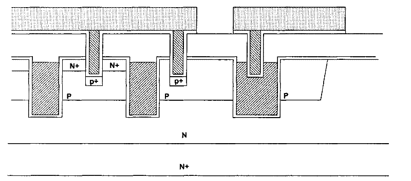
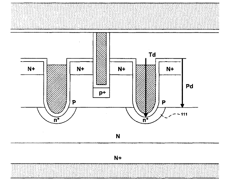
[0056] The invention is explained in more detail below with reference to the accompanying drawings, in which preferred embodiments of the invention are shown. The invention can, however, be embodied in different ways and should not be limited to the embodiments described herein. For example, the description here refers more to N-channel trench MOSFETs, but clearly other devices are possible.

[0057] refer to Figure 5 In a preferred embodiment of the present invention shown, an N-type epitaxial layer 201 is formed on an N+ substrate 200, and the inner surface of a trench formed in the epitaxial layer is lined with a gate oxide 220 and filled with doped The polysilicon respectively forms the first trench gate 210 in the active region and the second trench gate 211 connected to the gate metal. Preferably, the width of the second trench gate 211 is greater than or equal to the width of the first trench gate 210 . Around the bottom of each trench gate 210 and 211 , and on the u...


PUM


Abstract

The invention discloses a trench metal-oxide-semiconductor field effect transistor (MOSFET) with a shallow trench structure and a manufacturing method thereof. Compared with the trench MOSFET in the prior art, the trench MOSFET with a shallow trench structure in the invention has smaller grid charge and lower source and drain resistance, and meanwhile, maintains the breakdown voltage required by the device. In some preferable embodiments, the upper surface of the conducting region in the trench grid, which is connected with the grid metal, is higher than the upper surface of the conducting region in the trench grid of the active region, thereby further avoiding the possible phenomenon of excessive etching in the etching process of the grid contact trench.

Description

technical field [0001] The invention relates to a unit structure, a device structure and a manufacturing process of a semiconductor power device. In particular, it relates to a novel cell and terminal structure of a trench MOSFET (Metal Oxide Semiconductor Field Effect Transistor) with a shallow trench structure, which has low source-drain resistance (Rds), low gate charge (Qg) and higher breakdown voltage (BV). In addition, the present invention particularly relates to an improved process for manufacturing such trench MOSFETs. Background technique [0002] In order to solve the problem that traditional trench MOSFETs usually have relatively high Qg, a trench MOSFET with a shallow trench structure is disclosed in the prior art, as shown in Figure 1, that is, the trench gate in the epitaxial layer The depth Td (such as figure 2 shown) is shallower than conventional trench MOSFETs, so the meaning of the term "shallow trench" will be clear to those of ordinary skill in the a...

Claims


Application Information

Patent Timeline
IPC IPC(8): H01L29/78H01L29/06H01L29/36H01L21/336
Inventor 谢福渊
Owner FORCE MOS TECH CO LTD
Why Eureka
Try Eureka