Trench MOSFET with implanted drift region

a drift region and mosfet technology, applied in the direction of semiconductor devices, electrical apparatus, transistors, etc., can solve the problems of epitaxial resistivity, further technical difficulties and limitations of device implementation, and device designers now face another technical difficulty, so as to reduce gate to drain capacitance and reduce rds. , the effect of further improving the performance of the devi

Active Publication Date: 2009-12-15
FORCE MOS TECH CO LTD
View PDF5 Cites 0 Cited by
  • Summary
  • Abstract
  • Description
  • Claims
  • Application Information

AI Technical Summary

Benefits of technology

[0009]Another aspect of this invention is to form an improved MOSFET device with thick either split gate or gate padded with thicker oxide layer at the bottom of the trenched gate such that the gate to drain capacitance can be reduced. The performance of the device is further improved with reduced Rds by reducing the resistivity of the epitaxial layer while implemented with tilt-angle implanted drift regions to prevent degraded breakdown voltage both in the active cell areas or in the termination area.
[0010]Another aspect of this invention is to form an improved MOSFET device with tilt-angle implanted drift regions for preventing degraded breakdown voltages with reduced epitaxial resistivity. A breakdown voltage of less than fifty volts can be implemented with regular field plate without requiring guard rings. A breakdown voltage of greater than fifty volts can be implemented with guard rings formed in the termination area. Additional performance is achieved with either a split gate or a gate with thicker bottom oxide layer and thinner upper gate layer.
[0011]Briefly in a preferred embodiment, this invention discloses a trenched semiconductor power device comprising a plurality of trenched gates surrounded by source regions near a top surface of a semiconductor substrate encompassed in body regions. The trenched semiconductor power device further includes tilt-angle implanted drift regions surrounding the trenched gate at a lower portion of the body regions for preventing a degraded breakdown voltage due to a reduced epitaxial resistivity of an epitaxial layer supported on the semiconductor substrate. In an exemplary embodiment, the semiconductor power device further includes a metal oxide semiconductor field effect transistor (MOSFET) device. In an exemplary embodiment, the semiconductor power device further includes a N-channel MOSFET device having N-type tilt-angle implanted drift regions in an N-epitaxial layer supported on a N+ substrate. In an exemplary embodiment, the semiconductor power device further includes a P-channel MOSFET device having P tilt-angle implanted drift regions in a P-epitaxial layer supported on a P+ type substrate. In another exemplary embodiment, the semiconductor power device further includes guard rings disposed at a termination area for operating at a breakdown voltage greater than fifty volts and in a range of approximately 50 to 200 volts. In another exemplary embodiment, the semiconductor power device further includes a field plate disposed at a termination area for operating at a breakdown voltage ranging between eight volts to fifty volts. In another exemplary embodiment, each of the trenched gates having a thicker oxide layer on sidewalls of a lower portion of the trenched gates and a thinner oxide layer on sidewalls at an upper portion of the trenched gates. In another exemplary embodiment, each of the trenched gates further includes a bottom portion having a smaller width and padded with a thicker gate oxide layer on sidewalls of the trenched gates and a top portion having a greater width and padded with a thinner gate oxide layer on sidewalls of the trenched gates. In another exemplary embodiment, the epitaxial layer having a resistivity ranging between 0.3 to 3.0 mohm-cm and the trenched semiconductor power device having a breakdown voltage ranging between 8 to 200 volts. In the active area, since the thick oxide thickness in the trench bottom and in the lower portion of the sidewalls ranging from 0.1 to 1.0 um, with the thickness of the oxide layer depending on the breakdown voltage, shares more than 50% voltage during reverse bias, the doping concentration of the implanted drift region is thus significantly enhanced without degrading the targeted breakdown voltage. In termination region, the lightly doped epi is able to support the target breakdown voltage using traditional terminations such as metal filed-plate, and combination of field plate with guard ring.

Problems solved by technology

However, a thicker oxide layer formed at the trench bottom may also cause further technical difficulties and limitations of device implementations.
Since the epitaxial layer has a resistivity that is significantly dropped in order to satisfy a design target of further reducing the Rds, the device designers now confront another technical difficulty.
With the reduction of the epitaxial resistivity, the edge trench filed plate may not support the requirement that the breakdown voltage in the termination area must be higher than edge trench field plate.
A degradation of the breakdown voltage is therefore becoming a design and operation limitation.
However, as discussed above, when the resistivity of the epitaxial layer is decreased to provide a low Rds, the trench field plate may not support the breakdown voltage.
Additional disclosures of similar technologies are also published by M. A. Gajda et al “Industrialisation of Resurf Stepped Oxide Technology for power Transistors” (Proceedings of the 18th International Symposium on Power Semiconductor Device and ICs Jun. 4-8 2006 ISPD 2006) However, the trenched filed plate termination may not support the targeted breakdown voltage due to the lower epitaxial resistivity than the conventional devices.

Method used


Image

  • Trench MOSFET with implanted drift region
  • Trench MOSFET with implanted drift region
  • Trench MOSFET with implanted drift region

Examples


Embodiment Construction

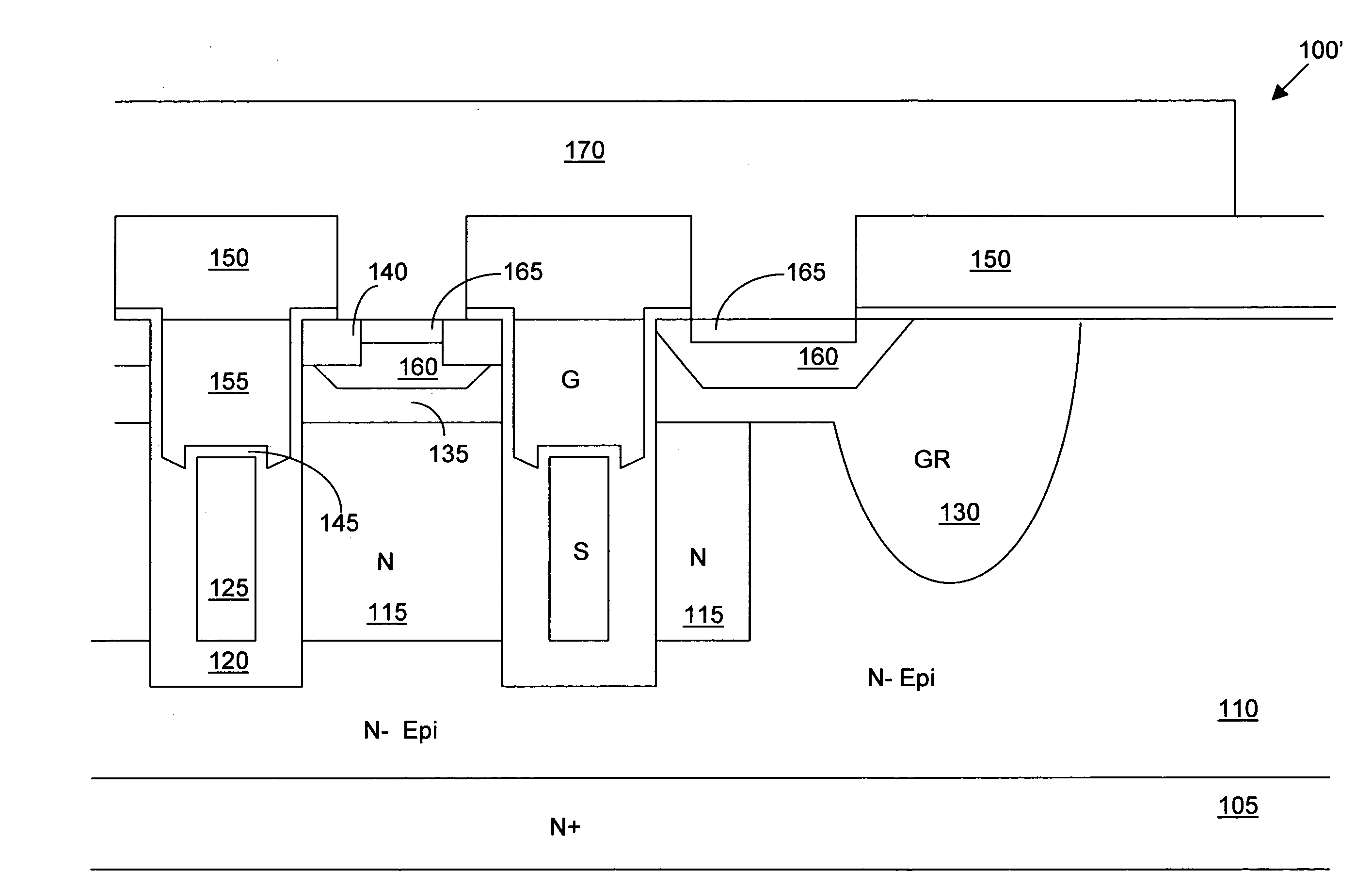
[0019]Referring to FIG. 2 for a side cross sectional view of a MOSFET device 100 formed on a N+ substrate 105 supporting an N-epitaxial layer 110 with trenched polysilicon gates. Each of these trenched gates includes a top gate segment 155 and a bottom gate segment 125 insulated by an inter-gate-segment oxide layer 145. The bottom gate segment 125 is padded by a thick oxide layer 120 and the top gate segment is padded by a normal gate oxide layer 145′ that is formed by the same oxide layer growth process as the inter-gate-segment insulation oxide 145. A plurality of P-body regions 135 surround the trenched gates that include the top and bottom gate segments 125 and 155 respectively. The body regions 135 further encompassed source regions 140 formed near the top surface of the epitaxial layer 110 surrounding the trenched gates. The areas on the top surface between adjacent source regions 140 are implemented as source contact surface. For the purpose of enhancing device ruggedness or ...


PUM


Abstract

A method to manufacture a trenched semiconductor power device including a plurality of trenched gates surrounded by source regions near a top surface of a semiconductor substrate encompassed in body regions. The method for manufacturing the trenched semiconductor power device includes a step of carrying out a tilt-angle implantation through sidewalls of trenches to form drift regions surrounding the trenches at a lower portion of the body regions with higher doping concentration than the epi layer for Rds reduction, and preventing a degraded breakdown voltage due to a thick oxide in lower portion of trench sidewall and bottom. In an exemplary embodiment, the step of carrying out the tilt-angle implantation through the sidewalls of the trenches further includes a step of carrying out a tilt angle implantation with a tilt-angle ranging between 4 to 30 degrees.

Description

BACKGROUND OF THE INVENTION[0001]1. Field of the Invention[0002]The invention relates generally to the device configuration and manufacturing methods for fabricating the semiconductor power devices. More particularly, this invention relates to an improved and novel manufacturing process and device configuration for providing the MOSFET device with implanted drifted region to prevent degraded breakdown voltages for both the active area and the termination area.[0003]2. Description of the Related Art[0004]In order to increase the switching speed of a semiconductor power device, it is desirable to reduce the electric charges between the gate and drain such that a reduction of a gate to drain capacitance Crss can be reduced. A thick oxide formed at the trench bottom of the trench gate is frequently implemented to reduce the gate to drain capacitance. However, a thicker oxide layer formed at the trench bottom may also cause further technical difficulties and limitations of device impleme...

Claims


Application Information

Patent Timeline
Patent Type & Authority Patents(United States)
IPC IPC(8): H01L29/76H01L31/062H01L31/113H01L31/119H01L29/94
CPCH01L29/0878H01L29/1095H01L29/7813H01L29/66734H01L29/7811H01L21/26586H01L29/0619H01L29/402H01L29/41741H01L29/42368H01L29/407
Inventor HSHIEH, FWU-IUAN
Owner FORCE MOS TECH CO LTD
Why Eureka
Try Eureka