NAND-based memory plate
A storage board and storage array technology, applied in the direction of input/output to record carrier, etc., can solve the problems of large equipment volume, power consumption, low storage bandwidth, etc., achieve high storage bandwidth, large storage capacity, and solve the effect of complex equipment
- Summary
- Abstract
- Description
- Claims
- Application Information
AI Technical Summary
Problems solved by technology
Method used
Image
Examples
Embodiment Construction
[0013] Below in conjunction with accompanying drawing and specific embodiment the present invention is described in further detail:
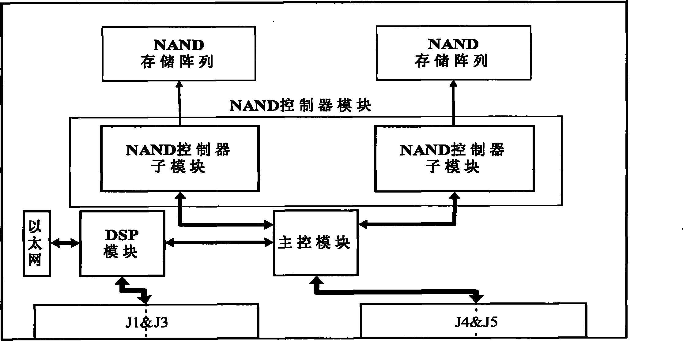
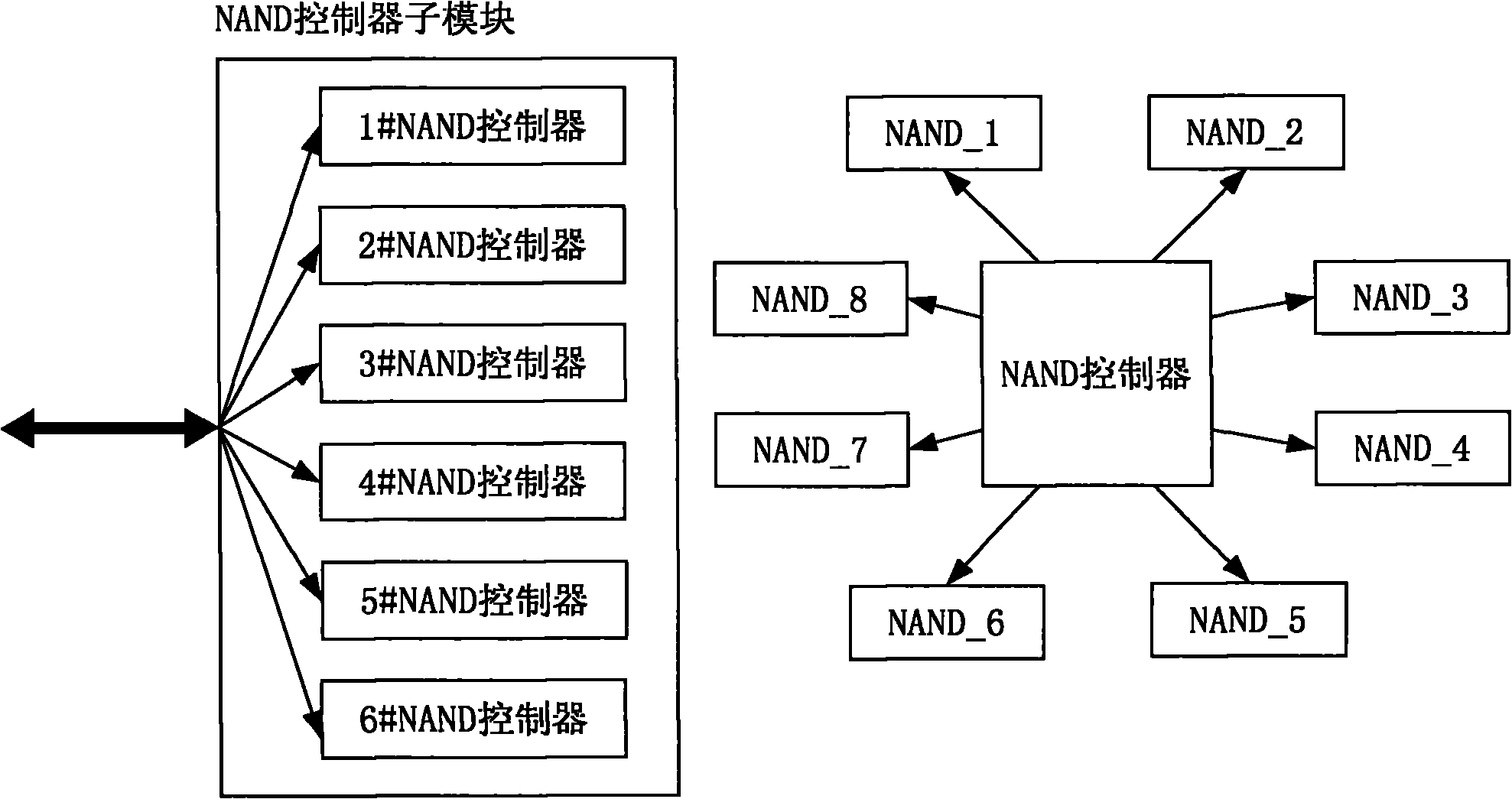
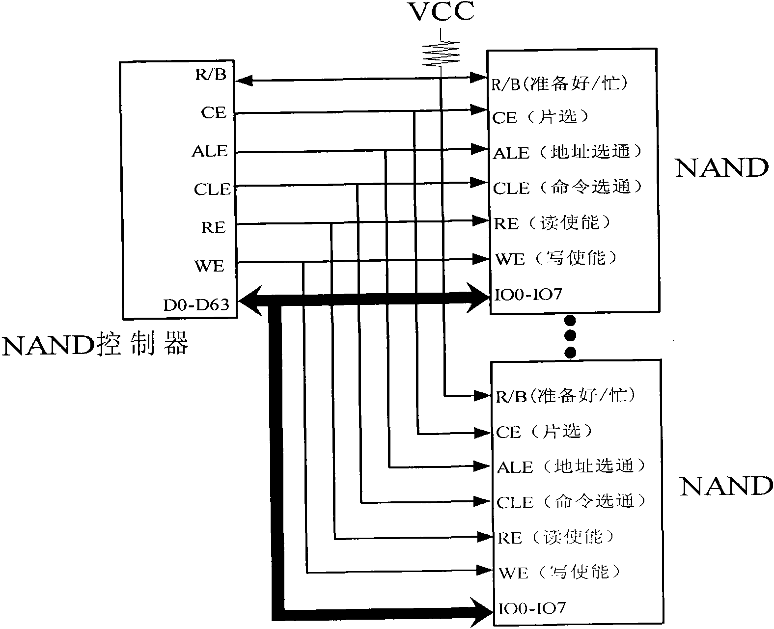
[0014] Such as figure 1 As shown, the whole board has a total of 96 K9WBG08U1M NAND chips (each chip has a storage capacity of 4GB), and each group of 8 chips is a group of 12 groups, which are connected to two groups of NAND controller sub-modules on average; each NAND controller sub-module It is realized by a piece of XC4VLX60FPGA of Xilinx Company, on which 6 groups of NAND controllers are designed to read and write access to 48 pieces of NAND in parallel, such as figure 2 shown. Each NAND controller manages 8 pieces of NAND, and the 6 control signals (CE, ALE, CLE, RE, WE, R / B) of the 8 pieces of NAND are connected together, and the data lines (8bit×8=64bit) are separated independently , so as to achieve parallel access to 8 pieces of NAND (such as image 3 shown). The NAND controller sub-module realizes data exchange with the main cont...
PUM
 Abstract
Description
Claims
Application Information
 - R&D
- Intellectual Property
- Life Sciences
- Materials
- Tech Scout
- Unparalleled Data Quality
- Higher Quality Content
- 60% Fewer Hallucinations
Browse by: Latest US Patents, China's latest patents, Technical Efficacy Thesaurus, Application Domain, Technology Topic, Popular Technical Reports.
© 2025 PatSnap. All rights reserved.Legal|Privacy policy|Modern Slavery Act Transparency Statement|Sitemap|About US| Contact US: help@patsnap.com


