


Quick Research
Generate reliable direction feasibility study reports for your R&D in just a few steps.

Technical Q&A
Discover and master advanced knowledge NOW. Basics, ideas, possibilities, all at once.

Find Solutions
As an expert in R&D theories, this can generate solutions to your technical problems instantly.

Evaluate Feasibility
Analyze your overall solution with one click, know your potential R&D risks in advance.

Monitor Landscape
Get weekly tech updates, stay abreast of the latest tech innovations and key insights.
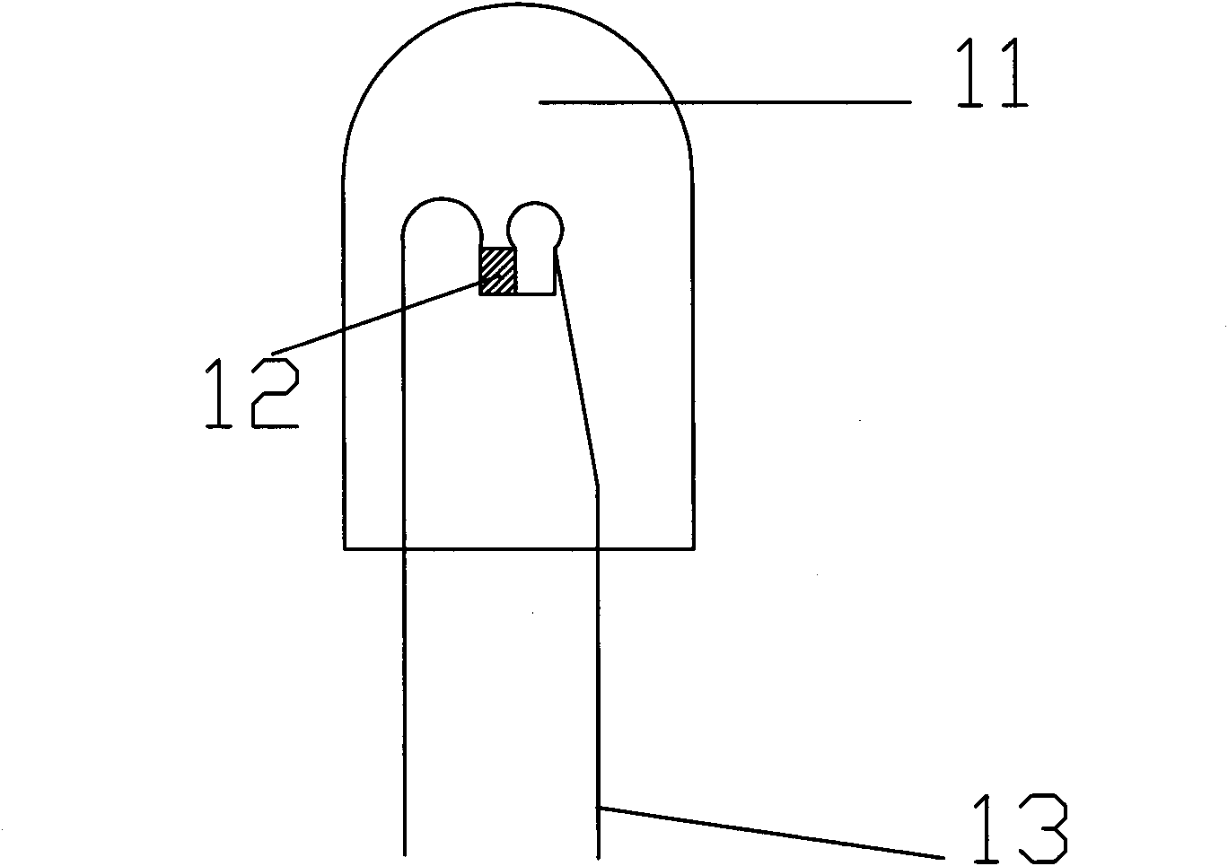
Packaging device of light-emitting diode and packaging method thereof
A technology for light-emitting diodes and packaging devices, applied in semiconductor devices, electrical components, circuits, etc., can solve the problems of limited thermal conductivity, easy accumulation, and thin electrode layer thickness, and achieve reliable insulation performance, good thermal matching performance, and heat dissipation performance. Good results
- Summary
- Abstract
- Description
- Claims
- Application Information
AI Technical Summary
Problems solved by technology
Method used
Image

Examples
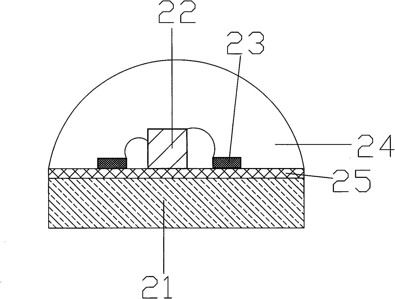
Embodiment 3
[0072] Preferably, the light-emitting diode packaging device of the third embodiment is manufactured by the following method during packaging, such as Figure 6 As shown, 122 in the figure is a glass-ceramic insulating layer, which is made by selective laser melting. 190 is a silver-plated heat conduction layer. The encapsulation method of implementing 3 comprises the following steps:
[0073] 1. Select a metal substrate 110, perform cleaning and degreasing treatment, and plate a 10-micron silver-plated heat-conducting layer on its front side.
[0074] 2. Drill out the required small holes on the silver-plated metal substrate 110 and perform cleaning treatment.
[0075] 3. Fabricate a mask on the front side of the metal substrate 110 to completely cover the front side.
[0076] 4. Put the masked metal substrate into an oxidation tank, and perform micro-arc oxidation or hard oxidation to form an aluminum oxide thin film insulation layer 121 with a thickness of more than 30 m...
PUM
 Abstract
Description
Claims
Application Information
 - R&D Engineer
- R&D Manager
- IP Professional
- Industry Leading Data Capabilities
- Powerful AI technology
- Patent DNA Extraction
Browse by: Latest US Patents, China's latest patents, Technical Efficacy Thesaurus, Application Domain, Technology Topic, Popular Technical Reports.
© 2024 PatSnap. All rights reserved.Legal|Privacy policy|Modern Slavery Act Transparency Statement|Sitemap|About US| Contact US: help@patsnap.com