
Nano-silicon thin-membrane four-island-beam-membrane sensor chip and preparation method thereof

A technology of nano-silicon thin film and membrane sensor, which can be used in instruments, manufacturing microstructure devices, piezoelectric devices/electrostrictive devices, etc., can solve problems such as difficult pressure measurement, and achieve the effect of improving sensitivity and linearity

Inactive Publication Date: 2010-12-22
JIANGSU UNIV
View PDF4 Cites 19 Cited by
  • Summary
  • Abstract
  • Description
  • Claims
  • Application Information

AI Technical Summary

Problems solved by technology

At present, the measurement range of this structure is only 300Pa, and it is difficult to measure even smaller pressures.

Method used


Image

  • Nano-silicon thin-membrane four-island-beam-membrane sensor chip and preparation method thereof
  • Nano-silicon thin-membrane four-island-beam-membrane sensor chip and preparation method thereof
  • Nano-silicon thin-membrane four-island-beam-membrane sensor chip and preparation method thereof

Examples


example

[0061] Example: Preparation of sensor chip

[0062] Use double-sided polished n-type (100) crystal orientation single crystal silicon wafer with a thickness of 200±10μm and a resistivity of 5-8Ω·cm. The chip manufacturing process is as follows:

[0063] 1. Thermal oxidation

[0064] A dry-wet-dry oxidation process is used to grow an oxide layer with a thickness of 100nm on the upper and lower surfaces of the silicon wafer. Oxidation temperature is 1150℃, dry oxygen for 10 minutes, steam wet oxygen for 30 minutes, and dry oxygen for 10 minutes.

[0065] 2. Double-sided lithography alignment mark

[0066] Double-sided photoetching of the oxidized silicon wafer to form double-sided alignment marks. Glue is applied on the back side, and the pre-baking temperature is 80°C for 8 minutes, and then the glue is applied on the front side, and the pre-baking temperature is 80°C, and the time is 15 minutes. Expose, develop and etch the alignment marks. (Simultaneously lithographically align the...


PUM

PropertyMeasurementUnit
sizeaaaaaaaaaa
thicknessaaaaaaaaaa
sizeaaaaaaaaaa

Abstract

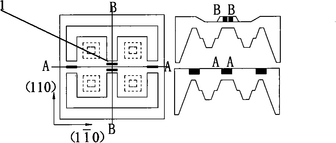
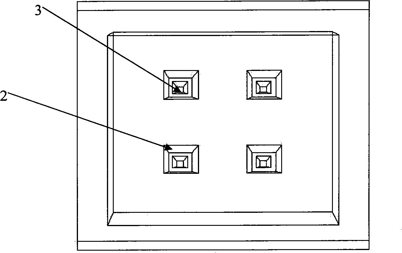
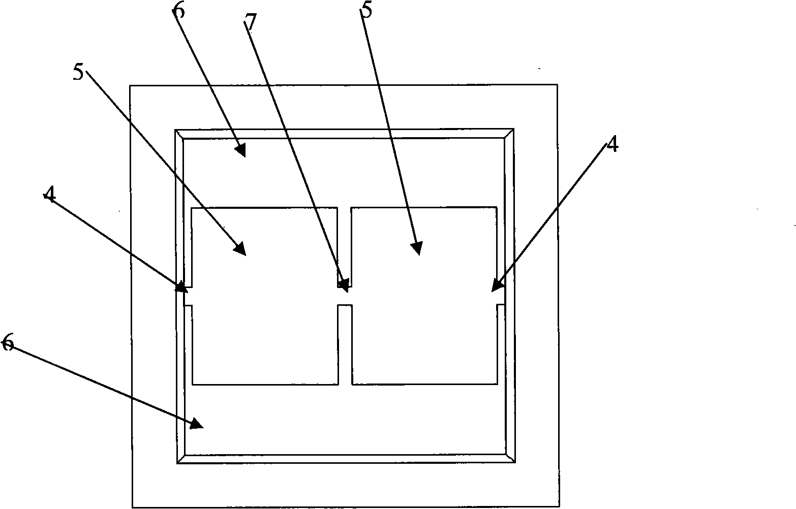
The invention relates to an ultra-micro pressure sensor, in particular to a nano-silicon thin-membrane four-island-beam-membrane sensor chip and a preparation method thereof. The sensor chip is square, monocrystalline silicon is adopted as a chip material, and nano-silicon is taken as a sensitive thin resistance material; the effective area of the chip is square, the back surface consists of four big islands and four small islands, and the small islands are positioned on the big islands; and the front surface of the effective chip area consists of a central beam, two edge beams, two flat membrane areas and two beam membrane areas, and resistors made of the nano-silicon material are arranged on the central beam and the edge beams. The sensor chip utilizes the advantages of a double-island beam membrane and combines the islands with the beams, thereby playing the effect of secondary stress concentration and improving the sensitivity and the linearity of a sensor; and the four resistors are respectively placed on the central beam and the edge beams, thereby transforming the stress of the resistors to the change of the resistance. The resistance change at the middle and the edges has the equal size and the reverse symbols, and the ultra-micro pressure measurement is realized by adopting the excitation of a constant current source through a Wheatstone bridge.

Description

Technical field [0001] The invention relates to an ultramicro pressure sensor, in particular to a nano silicon film four-island-beam-membrane sensor chip and a preparation method thereof. Background technique [0002] With the rapid development of science and technology, pressure testing technology has become more and more widely used in aerospace, aviation, transportation, metallurgy, machinery manufacturing, petrochemical, light industry, technical supervision and testing and other technical fields. Industrial automation, environmental protection equipment, and medical instruments all put forward an urgent need for the measurement of ultra-micro pressure, so the research on ultra-micro pressure sensors can have important significance and obvious value. [0003] At present, more than 80% of the high-performance pressure sensors used in the above-mentioned industries rely on imports and spend a lot of national foreign exchange every year. The purpose of the present invention is to...

Claims


Application Information

Patent Timeline
Patent Type & Authority Applications(China)
IPC IPC(8): G01L1/22G01L9/04B81B3/00B81C1/00
Inventor 丁建宁沈思国范真程广贵潘海彬范慧娟
Owner JIANGSU UNIV
Learn More