Light-emitting diode (LED) electrode structure for effectively utilizing current and manufacturing method thereof

A technology of electrode structure and manufacturing method, which is applied in the direction of circuits, electrical components, semiconductor devices, etc., can solve the problems of light shading, ineffective use of injected current, large chip area ratio, etc., to achieve simple operation, improve LED luminous efficiency, and reliability The effect of high sexual stability

Inactive Publication Date: 2010-12-08
Shandong Huaguang Optoelectronics Co. Ltd.
View PDF4 Cites 3 Cited by
  • Summary
  • Abstract
  • Description
  • Claims
  • Application Information

AI Technical Summary

Problems solved by technology

Although these designs can play a good role in current expansion, the first electrode 1 occupies a large proportion of the chip area, so a considerable part of the current is still concentrated under the first electrode 1, and the traditional LED electrode material is Opaque metal or metal alloy, which causes most of the light emitted from the bottom of the first electrode 1 to be blocked, and the injected current cannot be effectively used, such as figure 2 The current spread of the LED electrode made by the conventional method shown

Method used


Image

  • Light-emitting diode (LED) electrode structure for effectively utilizing current and manufacturing method thereof
  • Light-emitting diode (LED) electrode structure for effectively utilizing current and manufacturing method thereof
  • Light-emitting diode (LED) electrode structure for effectively utilizing current and manufacturing method thereof

Examples


Embodiment Construction

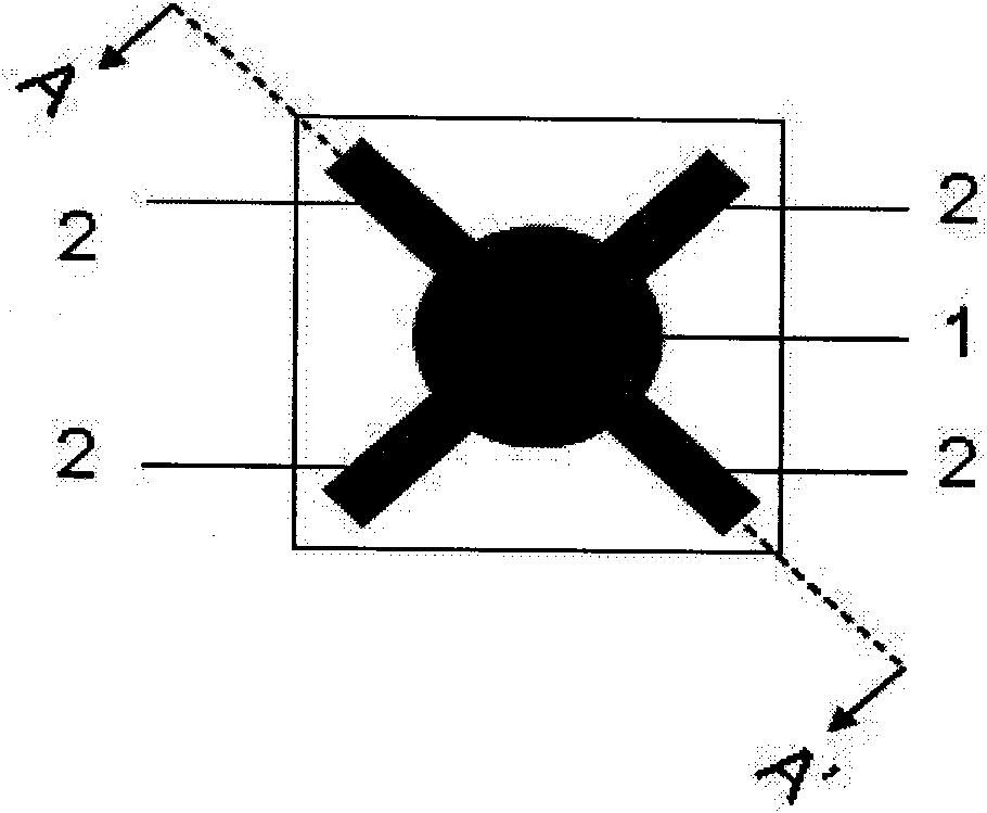
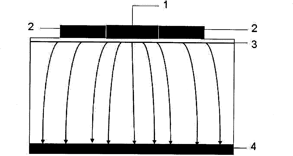
[0020] The LED electrode structure for effective current utilization of the present invention is that a part of the non-ohmic contact area is provided under the LED electrode. the following to figure 1 The known cross-shaped electrode shown is taken as an example to illustrate the LED electrode manufacturing method of the present invention.

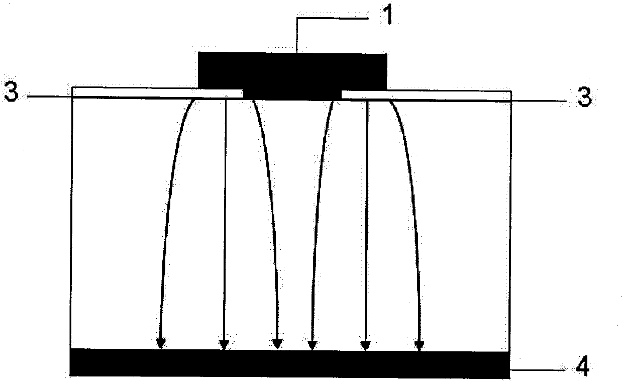
[0021] First, in image 3 On the ohmic contact layer 3 of the LED shown, the pattern of the part of the ohmic contact layer 3 to be removed is photoetched at the position where the first electrode 1 is to be made, and then this part of the ohmic contact layer is removed by a conventional wet or dry method. The material of the contact layer can be gallium phosphide, gallium arsenide, gallium nitride, gallium arsenide phosphide, gallium phosphide nitride, etc. Taking gallium arsenide as an example, put the chip into the volume ratio of hydrogen peroxide: ammonia water: water = 1: Shake up and down in the 5:1 gallium arsenide etching solut...


PUM


Abstract

The invention discloses a light-emitting diode (LED) electrode structure for effectively utilizing current and a manufacturing method thereof. In the LED electrode structure, a partial non-ohmic contact area is formed below an LED electrode. The method for manufacturing the LED electrode structure comprises the following steps of: manufacturing an ohmic contact layer on an LED tube core, removing a partial non-ohmic contact layer at a position, at which the electrode is to be manufactured, on the ohmic contact layer, removing a photoresist and washing, evaporating and coating a metal electrode layer on the entire ohmic contact layer including the removed part by the conventional method, and removing a part of metal electrode layer outside an electrode pattern to be manufactured by corroding; and alloying to form ohmic contact on the remaining ohmic contact layer. The LED electrode structure has the advantages of reducing blocked light, increasing effective utilization of current and improving luminous efficiency. The manufacturing method has the advantages of simple operation, easy implementation, high reliability and stability and wide application range.

Description

technical field [0001] The invention relates to an electrode manufacturing method of a semiconductor light-emitting diode (LED), belonging to the technical field of semiconductor device manufacturing. Background technique [0002] LED has many advantages such as high luminous efficiency, low power consumption, long life, low heat generation, small size, environmental protection and energy saving, so it has a wide range of application markets, such as automobiles, backlights, traffic lights, large-screen displays, military and other fields . [0003] With the rapid development of semiconductor technology, the internal quantum efficiency reaches more than 90%, while the external quantum efficiency is not significantly improved by many factors, such as chip structure and electrode shape, which directly affect the light extraction efficiency of LED. For an LED with a common structure, its structure includes from top to bottom: an upper electrode, an ohmic contact layer, a curre...

Claims


Application Information

Patent Timeline
Patent Type & Authority Applications(China)
IPC IPC(8): H01L33/38
Inventor 张秋霞徐现刚夏伟苏建陈康
Owner Shandong Huaguang Optoelectronics Co. Ltd.
Why Eureka
Try Eureka