Method for filling silicon through holes by using carbon nanotube clusters

A technology of carbon nanotubes and through-silicon vias, which is applied in the field of interconnection technology, can solve problems such as the difficulty in the number of transistors, achieve the effect of reducing size, reducing package size, and meeting high-density packaging

Active Publication Date: 2012-06-27
SHANGHAI SHANG DA RUI HU MICROSYST INTEGRATION TECH CO LTD SMIT
View PDF0 Cites 0 Cited by
  • Summary
  • Abstract
  • Description
  • Claims
  • Application Information

AI Technical Summary

Problems solved by technology

In recent years, it has become increasingly difficult to increase the number of transistors on a chip at the rate described by Moore's Law due to the constraints of fundamental physical laws

Method used


Image

  • Method for filling silicon through holes by using carbon nanotube clusters
  • Method for filling silicon through holes by using carbon nanotube clusters
  • Method for filling silicon through holes by using carbon nanotube clusters

Examples


Embodiment 1

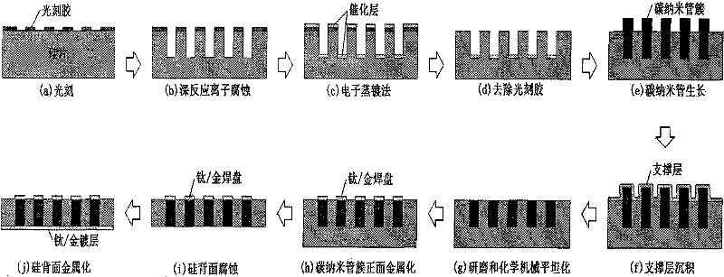
[0024] In this embodiment, the above-mentioned steps are used to prepare TSVs filled with carbon nanotube clusters, and the specific steps are as follows:

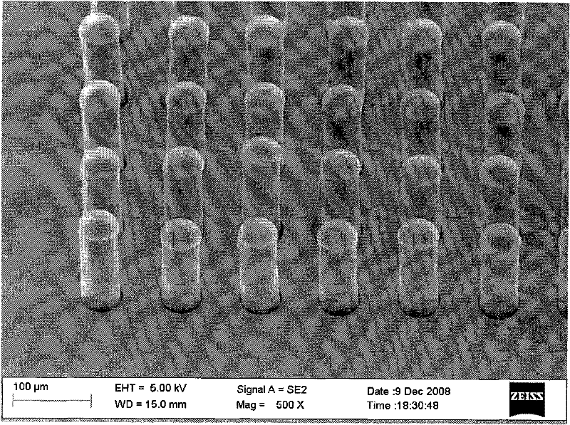
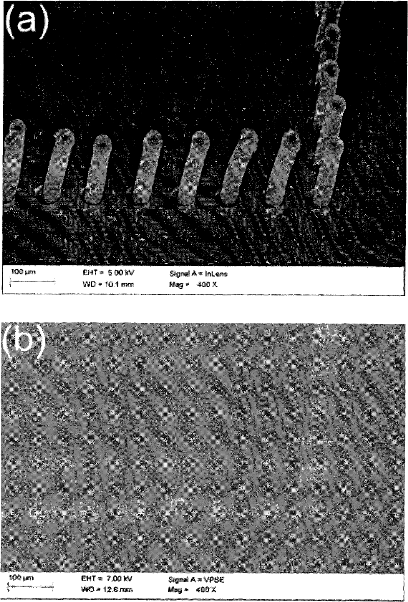
[0025] 1. First, use photolithography and deep reactive ion etching to manufacture a hole array with a diameter of 20 microns and a hole depth of 131 microns on a silicon wafer with a thickness of 7.62 cm. In the photolithography process, the photolithography covering the silicon surface The glue is not removed yet.

[0026] 2. Deposit a catalytic layer consisting of 10 nanometer thick Al2O3 and 1 nanometer thick iron on the silicon wafer by electron beam evaporation.

[0027] 3. Use isopropanone and deionized water to wash off the photoresist and the catalytic layer on the photoresist. At this time, only the bottom of the hole remains with the catalytic layer.

[0028] 4. Put the silicon wafer into a quartz tube with a diameter of 4 cm and a length of 50 cm. Argon gas of 900 sccm and hydrogen gas of 100 sccm were passed...


PUM

PropertyMeasurementUnit
thicknessaaaaaaaaaa
thicknessaaaaaaaaaa
thicknessaaaaaaaaaa

Abstract

The invention discloses a method for filling silicon through holes by using carbon nanotube clusters in microelectronic packaging. The method comprises the following steps of: making holes in specific shapes and management on a silicone chip by using photoetching technology and deep reactive ion etching technology; depositing a catalyst layer consisting of aluminium oxide and iron on the bottoms of the holes; under the conditions of certain gas flow and temperature, growing the carbon nanotube clusters from the bottoms of the holes; sputtering a support layer consisting of silicon and a photoresist on the upper surface of the silicon chip and the surfaces of the carbon nanotube clusters; grinding by using grinding and chemical mechanical planarization methods to obtain flat and neat surfaces of the carbon nanotube clusters and surface of the silicon chip; plating a titanium / gold metal film serving as a pad on the surfaces of the carbon nanotube clusters; removing the silicon on the back of the silicon chip until the bottoms of the carbon nanotube clusters are exposed; and finally, plating a titanium / gold metal film on the back of the silicon chip to obtain the silicon through holes filled with the carbon nanotube clusters. Through the method, the silicon through holes with the pore diameter of about 20 micrometers can be obtained, and the requirements on density and miniaturization of electronic devices in the future are met.

Description

technical field [0001] The invention relates to an interconnection technology for microelectronic packaging, which is mainly applied to the packaging form of three-dimensional stacked chips. Specifically, it is a method of filling through-silicon holes with carbon nanotube clusters. Background technique [0002] For decades, the general trend in the development of electronic products has been to achieve greater speed and more functions in ever-shrinking product sizes. This is mainly achieved in two ways. One is to continuously integrate more transistors on the chip to increase the computing speed, increase the storage space, and realize more functions. According to the famous "Moore's Law", the number of transistors that can be integrated on a chip with the same area doubles every eighteen to twenty-four months. The second is to integrate more devices in products through various high-density packaging technologies. In recent years, it has become increasingly difficult to...

Claims


Application Information

Patent Timeline
Patent Type & Authority Patents(China)
IPC IPC(8): H01L21/60
CPCB82Y10/00H01L2221/1094H01L29/0676H01L2924/00013H01L21/76898B82Y40/00
Inventor 刘建影张霞王腾张燕
Owner SHANGHAI SHANG DA RUI HU MICROSYST INTEGRATION TECH CO LTD SMIT
Why Eureka
Try Eureka