Radiating fin and semiconductor packaging structure

A heat sink and semiconductor technology, applied in semiconductor devices, semiconductor/solid-state device parts, electric solid-state devices, etc., can solve the problems of heat sink and substrate position offset, increasing the difficulty of substrate design and production, occupying design area, etc.

Inactive Publication Date: 2010-10-13
ADVANCED SEMICON ENG INC
View PDF0 Cites 3 Cited by
  • Summary
  • Abstract
  • Description
  • Claims
  • Application Information

AI Technical Summary

Problems solved by technology

Although in this kind of semiconductor chip packaging structure, the heat sink can be positioned on the substrate by fitting the second fitting portion into the first fitting portion, but the first fitting such as a cavity is provided on the substrate. part must change the design of the substrate, and the first fitting part will occupy the design area of ​​the circuit of the substrate, so when the area of ​​the substrate and the pitch of the circuit are gradually reduced, it will increase the difficulty of designing and manufacturing the substrate
[0006] Therefore, there is still a need to provide a new heat sink structure to solve the problem of positional offset between the heat sink and the substrate in the prior art

Method used


Image

  • Radiating fin and semiconductor packaging structure
  • Radiating fin and semiconductor packaging structure
  • Radiating fin and semiconductor packaging structure

Examples


Embodiment Construction

[0036] In order to make the above and other objects, features, and advantages of the present invention more apparent, the embodiments of the present invention, together with the attached figures, are described in detail below.

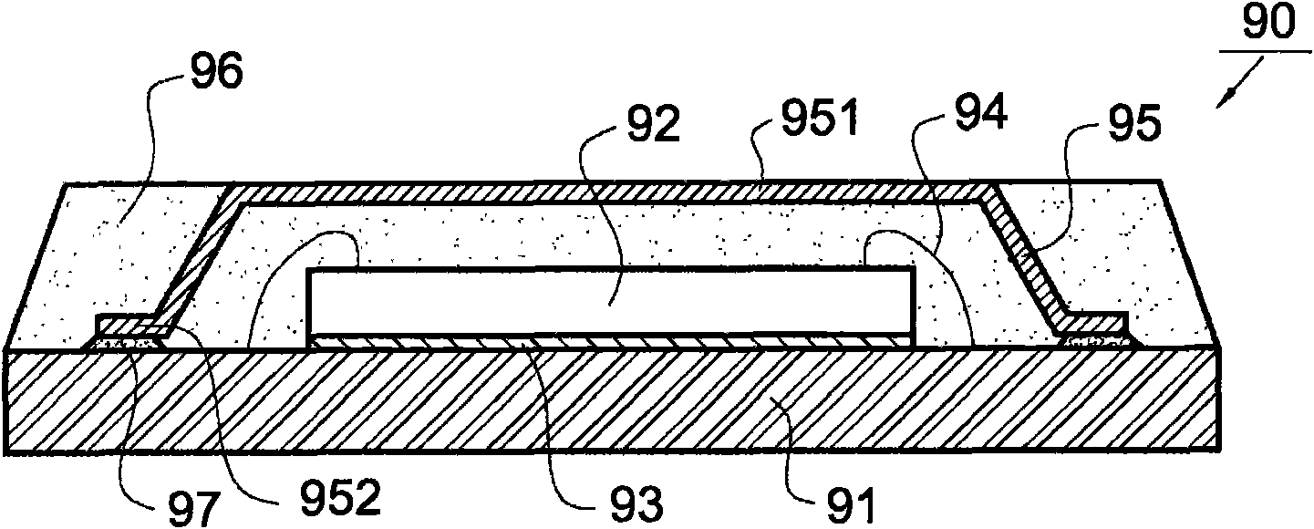
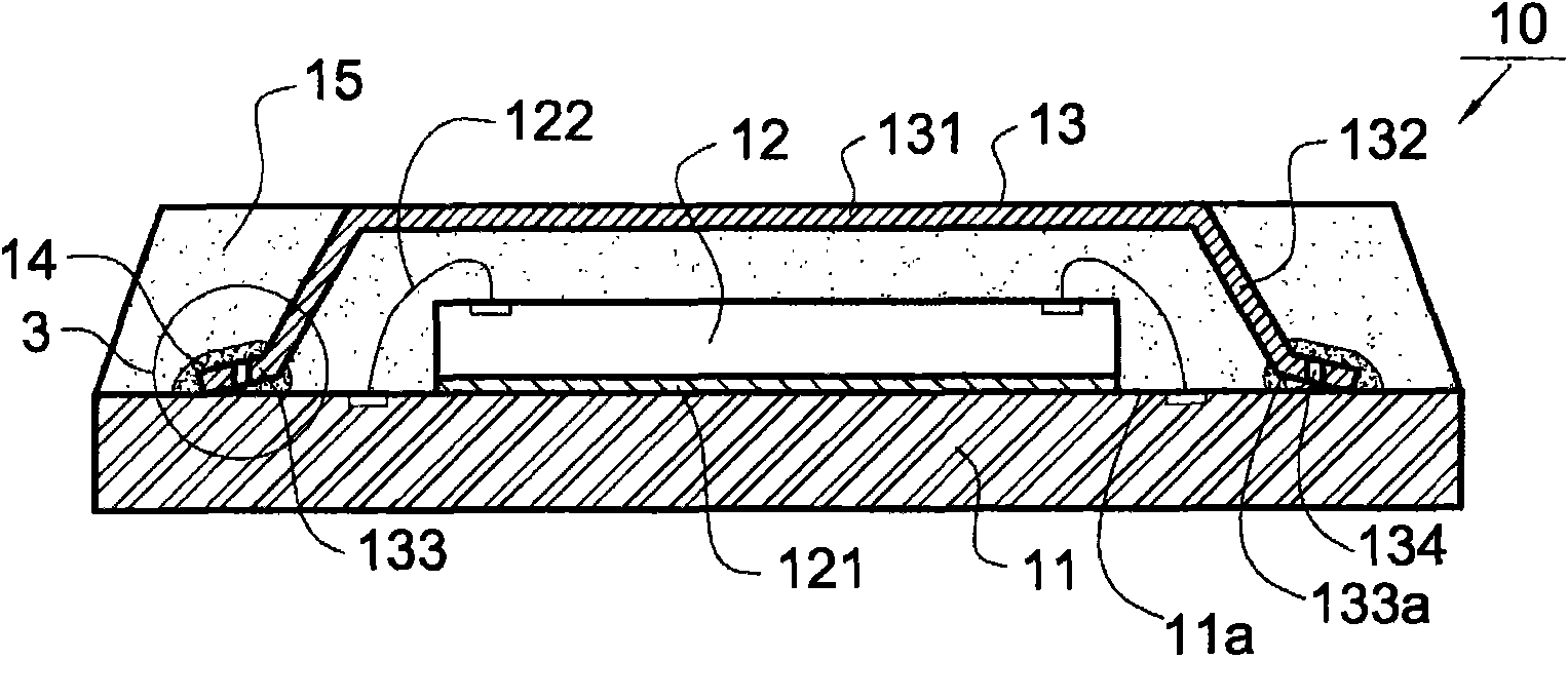
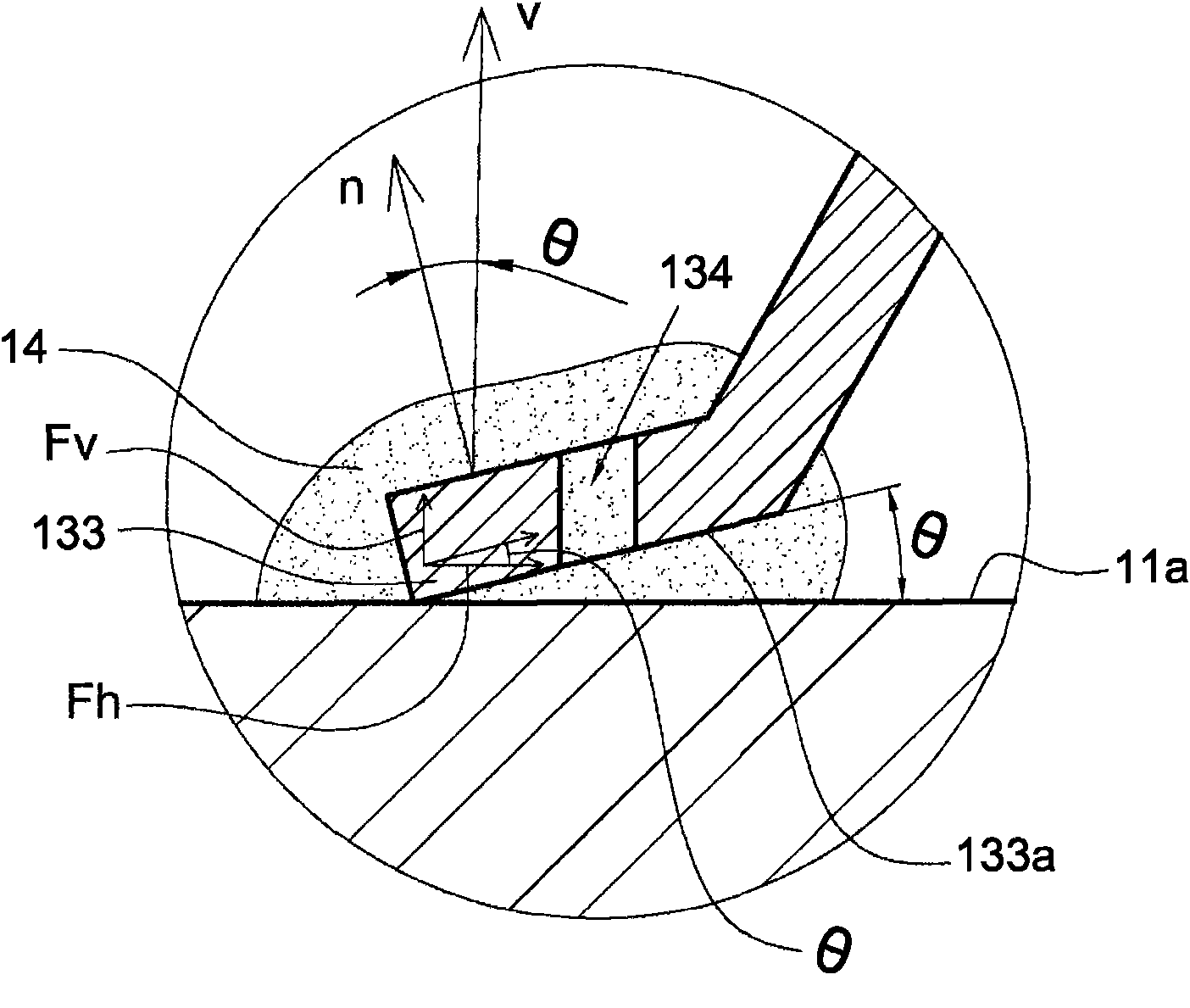
[0037] Please refer to figure 2 As shown, it shows a cross-sectional view of a semiconductor package structure 10 according to an embodiment of the present invention. The semiconductor package structure 10 includes a chip carrier 11 , a chip 12 , a heat sink 13 , an adhesive 14 and an encapsulant 15 . The chip carrier 11 can be a substrate, for example, which includes an upper surface 11a for carrying the chip 12 and the heat sink 13, and the upper surface 11a of the chip carrier 11 includes several pads (not shown) and circuit structures. (not shown).

[0038] The chip 12 is glued on the chip carrier 11 by a die-bonding glue 121, and the active surface of the chip 12 includes several welding pads (not shown), which are electrically connected to the ...


PUM


Abstract

The invention relates to a radiating fin, comprising a radiating part and a supporting part. The supporting part extends along the direction far away from the radiating part from the edge of the radiating part; the tip of the supporting part is provided with a plurality of butting parts, wherein, each butting part is provided with a bottom surface; and the normal direction and the vertical direction of the bottom surface form an angle which is more than 5 degrees. The invention further provides a semiconductor packaging structure.

Description

technical field [0001] The invention relates to a semiconductor packaging component, in particular to a heat sink and a semiconductor packaging structure. Background technique [0002] As the operating speed of the chip is increasing day by day, how to effectively remove the huge heat energy generated during the operation of the chip is an important issue in the semiconductor packaging structure when the chip is packaged. The heat sink has a simple process and can achieve the purpose of heat dissipation. [0003] Please refer to figure 1 As shown, it shows a conventional semiconductor package structure 90 with a heat sink, which includes a substrate 91, a chip 92, a die-bonding glue 93, several bonding wires 94, a heat sink 95 and a sealant 96 . The chip 92 is adhered on the substrate 91 through the die-bonding glue 93 , and is electrically connected to the substrate 91 through the bonding wires 94 . The heat sink 95 is disposed above the chip 92 and adhered to the subst...

Claims


Application Information

Patent Timeline
Patent Type & Authority Applications(China)
IPC IPC(8): H01L23/40H01L23/13
CPCH01L2924/0002H01L2224/48091H01L2224/73265
Inventor 张云龙丘彬鸿刘俊成
Owner ADVANCED SEMICON ENG INC
Why Eureka
Try Eureka