Method of transferring device
A device, horizontal technology, applied in the field of transfer devices, can solve problems such as uneven pressure
- Summary
- Abstract
- Description
- Claims
- Application Information
AI Technical Summary
Problems solved by technology
Method used
Image
Examples
no. 1 example
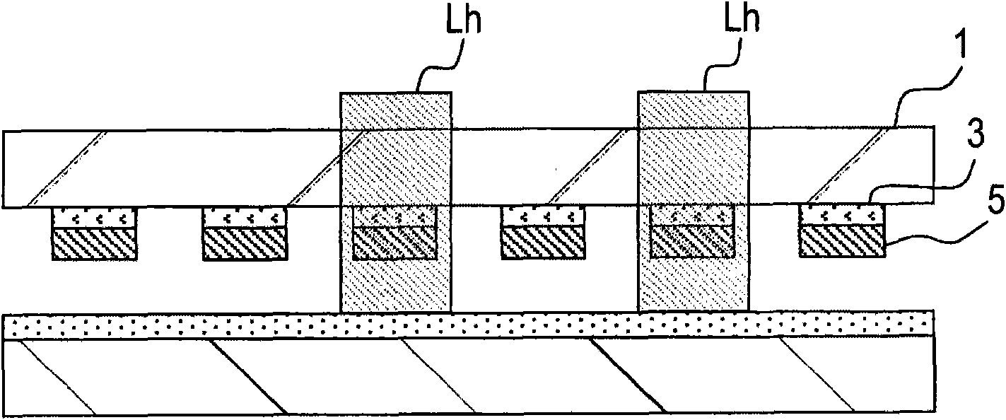
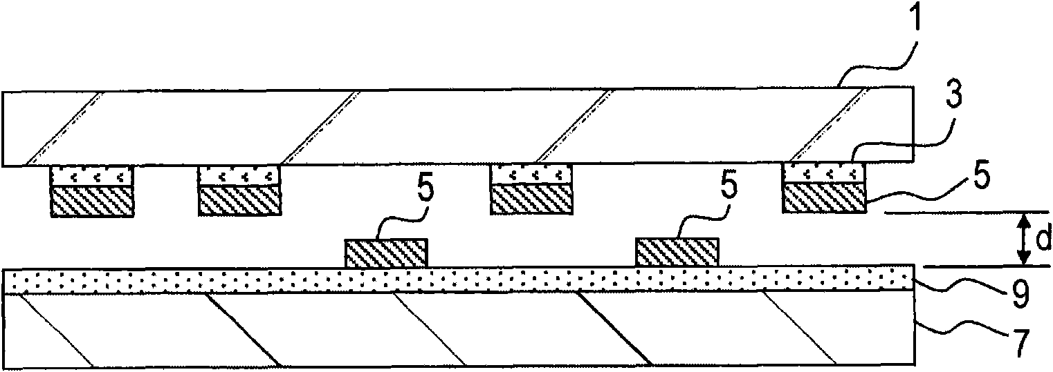
[0029] Figure 1A ~ Figure 1D is a cross-sectional processing diagram showing a method of transferring a device using the present invention. The method of transferring devices described here is, for example, a method of transferring LED devices from a first substrate to a second substrate in a manufacturing process of a display device in which light emitting diodes (LEDs) are arranged in a matrix, or the like. The method is carried out as follows.
[0030] First, if Figure 1A As shown, a plurality of devices 5 are located on the first substrate 1 , and the release layer 3 is sandwiched between the devices 5 and the first substrate 1 . The adhesive layer 9 is disposed on the second substrate 7 .
[0031] The first substrate 1 is, for example, a substrate on which devices constituting a display device are mounted. The first substrate 1 is made of a material that does not absorb the laser beam used in the transfer method, and the material makes it possible to observe the devi...
no. 2 example
[0064] refer to Figure 3A ~ Figure 4D , as a second embodiment, a method of repairing a device regarding the transfer of a missing portion of the device from a first substrate to a second substrate will be described.
[0065] like Figure 3A floor plan and Figure 3B The section view (corresponding to the Figure 3A As shown in the cross-section shown by line A-A' of ), the devices 5 are transferred onto the second substrate 7 in a predetermined arrangement through the steps of the first embodiment or other steps. In this case, there is a device-missing portion B in which the device 5 is not transferred on the second substrate 7, and the device 5 is transferred relative to the device-missing portion B, thereby performing repair.
[0066] In this case, first, if Figure 4A As shown, a new first substrate 1 mounted with devices 5 for repair is arranged opposite to a second substrate 7 on which a plurality of devices 5 have already been transferred. In this case, similarly ...
no. 3 example
[0076] refer to Figure 5 and FIG. 6 , as a third embodiment, illustrates a first example in which the arrangement of the first substrate is changed and devices are rearranged on the second substrate. In this case, the transition when the characteristics of the device columns are averaged will be described.
[0077] Figure 5 A case where a plurality of light emitting devices 5 are mounted on the first substrate 1 and a case where the luminous intensity is distributed are shown. This luminous intensity distribution originates from the distribution on the wafer on which the light emitting device 5 is formed.
[0078] In this case, first, if Figure 6A As shown in (1), alternately arranged devices 5 are transferred from the first substrate 1 to the first transfer range A on the second substrate. Then, if Figure 6A As shown in (2), at the position where the transfer range A is shifted in the horizontal direction by half with respect to A in the +x direction, the second tran...
PUM
 Abstract
Description
Claims
Application Information
 - R&D Engineer
- R&D Manager
- IP Professional
- Industry Leading Data Capabilities
- Powerful AI technology
- Patent DNA Extraction
Browse by: Latest US Patents, China's latest patents, Technical Efficacy Thesaurus, Application Domain, Technology Topic, Popular Technical Reports.
© 2024 PatSnap. All rights reserved.Legal|Privacy policy|Modern Slavery Act Transparency Statement|Sitemap|About US| Contact US: help@patsnap.com


