Array substrate, manufacturing method thereof and wide-viewing angle liquid crystal display
A technology of array substrate and substrate substrate, which is applied in semiconductor/solid-state device manufacturing, instruments, electric solid-state devices, etc., can solve the problems of increasing equipment investment, and achieve the effects of small equipment investment, reduction of storage capacitance, and cost reduction.
- Summary
- Abstract
- Description
- Claims
- Application Information
AI Technical Summary
Problems solved by technology
Method used
Image

Examples
no. 1 example
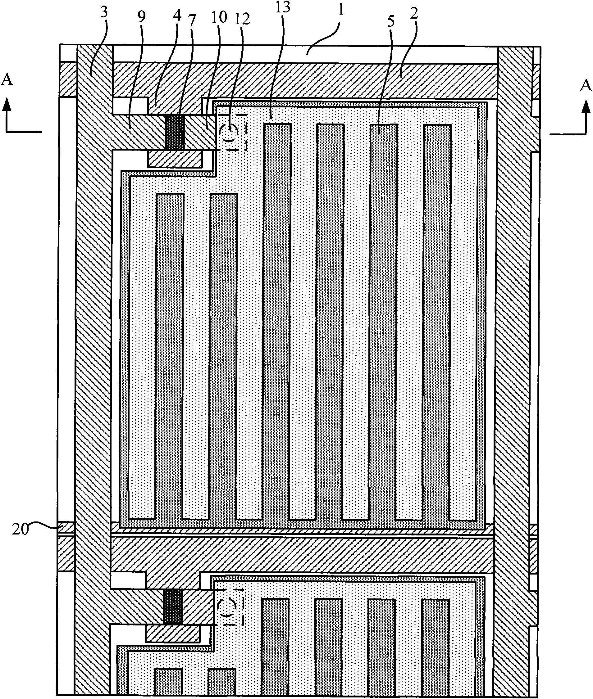
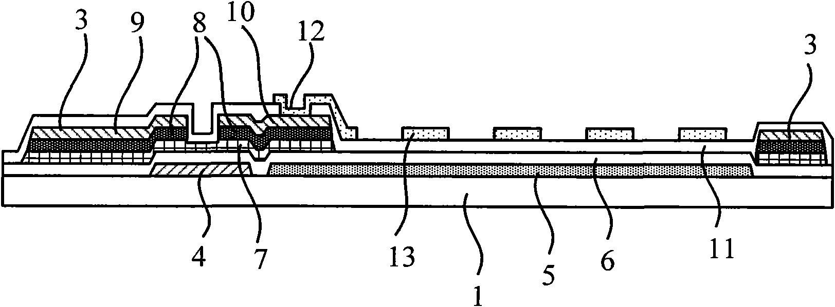
[0034] image 3 It is a schematic cross-sectional structure diagram of the array substrate provided by the first embodiment of the present invention, and its partial top view structure schematic diagram can be found in figure 1 As shown (the gate insulating layer, passivation layer and organic transparent insulating layer are not shown in the plan view herein). The array substrate is specifically an array substrate in an FFS mode liquid crystal display, such as image 3 As shown, its specific structure includes: a base substrate 1, usually made of glass; a plurality of data lines 3 and gate lines 2 crossing each other are formed on the base substrate 1, and the data lines 3 and gate lines 2 define a A plurality of pixel areas arranged in matrix form; each pixel area includes common electrode lines 20, common electrodes 5, TFT switches, passivation layers 11 and pixel electrodes 13, and each pixel area is covered with a whole block of common electrodes 5. Corresponding to the...
no. 2 example
[0048] Figure 4 It is a flow chart of the manufacturing method of the array substrate provided by the second embodiment of the present invention, and the method specifically includes the following steps:
[0049] Step 100, using a patterning process on the base substrate to form patterns of common electrodes, common electrode lines, and TFT switches;
[0050] Step 200, a passivation layer may be deposited on the above-mentioned base substrate by PECVD method;
[0051] Step 300, forming an organic transparent insulating layer on the passivation layer, and using a patterning process to etch on the organic transparent insulating layer to form organic layer via holes, and simultaneously etch the passivation layer to form passivation layer via holes, the organic layer The via hole completely overlaps the passivation layer via hole;
[0052] Step 400, deposit a transparent conductive film layer on the organic transparent insulating layer, and use a patterning process to etch to f...
no. 3 example
[0055] Figure 5 It is a flow chart of the manufacturing method of the array substrate provided by the third embodiment of the present invention, and the method specifically includes the following steps:
[0056] Step 100, using a patterning process on the base substrate 1 to form the patterns of the common electrode 5, the common electrode line 20 and the thin film transistor switch;
[0057] A specific implementation of step 100 is as follows:
[0058] Step 101a, deposit a transparent conductive film layer on the base substrate 1, and use a patterning process to etch to form a pattern of the common electrode 5, such as Figure 6 and Figure 7 shown;
[0059] Step 102a, deposit a gate metal layer on the above-mentioned substrate 1, and use a patterning process to etch to form the pattern of the common electrode line 20, the gate line 2 and the gate electrode 4, as Figure 8 and Figure 9 shown;
[0060] Step 103a, depositing a gate insulating layer 6 on the above-mentio...
PUM
| Property | Measurement | Unit |
|---|---|---|
| Thickness | aaaaa | aaaaa |
| Thickness | aaaaa | aaaaa |
Abstract
Description
Claims
Application Information
 - Generate Ideas
- Intellectual Property
- Life Sciences
- Materials
- Tech Scout
- Unparalleled Data Quality
- Higher Quality Content
- 60% Fewer Hallucinations
Browse by: Latest US Patents, China's latest patents, Technical Efficacy Thesaurus, Application Domain, Technology Topic, Popular Technical Reports.
© 2025 PatSnap. All rights reserved.Legal|Privacy policy|Modern Slavery Act Transparency Statement|Sitemap|About US| Contact US: help@patsnap.com