Semiconductor device
A semiconductor and wiring technology, applied in the direction of semiconductor devices, semiconductor/solid-state device parts, electric solid-state devices, etc., can solve problems such as cracks in the connection parts, weakened connection strength of solder bumps, etc., achieve high production efficiency, miniaturization and Thinner, Higher Reliability Effects
- Summary
- Abstract
- Description
- Claims
- Application Information
AI Technical Summary
Problems solved by technology
Method used
Image
Examples
Embodiment 1
[0076] A semiconductor device according to Embodiment 1 of the present invention will be described with reference to the drawings. figure 1 It is a cross-sectional view schematically showing the structure of the semiconductor device according to Embodiment 1 of the present invention.
[0077] The semiconductor device 1 of the first embodiment is a package in which a semiconductor element 12 is embedded in a wiring substrate (support substrate 11 , buried insulating layer 13 , and fan-out wiring (Fan out wiring) 14 ). The semiconductor device 1 has a wiring thickness reinforcing portion 15 in a predetermined region above the outer peripheral portion of the semiconductor element 12 for preventing cracks in the embedded insulating layer 13 on the outer peripheral portion of the semiconductor element 12 .
[0078] The semiconductor element 12 is a semiconductor chip (for example, a silicon semiconductor element, etc.), and a plurality of pads (not shown) are provided on one surfac...
Embodiment 2
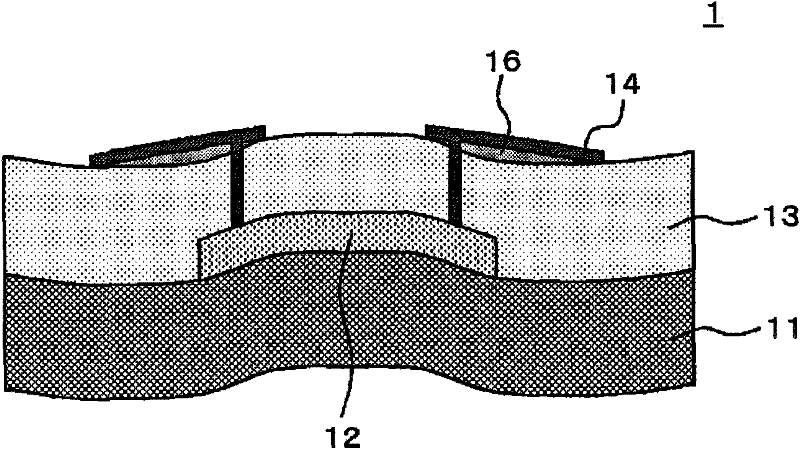
[0090] A semiconductor device according to Embodiment 2 of the present invention will be described with reference to the drawings. figure 2 It is a cross-sectional view schematically showing the structure of a semiconductor device according to Embodiment 2 of the present invention.
[0091] In the semiconductor device of Embodiment 2, instead of the wiring thickness reinforcing portion ( figure 1 The insulating layer thickness reinforcing portion 16 in 15) is used to prevent cracks in the embedded insulating layer 13 on the outer peripheral portion of the semiconductor element 12 . The insulating layer thickness reinforced portion 16 is arranged between the embedded insulating layer 13 and the fan-out wiring 14 . Other structures are the same as in Embodiment 1.
[0092] The insulating layer thickness reinforced portion 16 is provided vertically above the outer peripheral portion of the semiconductor element 12 and may be formed of an insulating material that forms an insul...
Embodiment 3
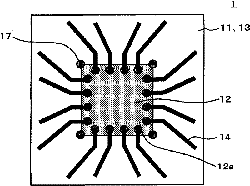
[0096] A semiconductor device according to Embodiment 3 of the present invention will be described with reference to the drawings. image 3 It is a cross-sectional view schematically showing the structure of a semiconductor device according to Embodiment 3 of the present invention.
[0097] The semiconductor device of Example 3 is a package in which a semiconductor element 12 is embedded in a wiring substrate (support substrate 11 , embedded insulating layer 13 , fan-out wiring 14 ). In order to prevent cracks in the buried insulating layer 13 on the outer peripheral portion of the semiconductor element 12, the semiconductor device 1 has a reinforcing via wiring 17 connected to at least one end (corner) of the semiconductor element 12 and not connected to the fan-out Wiring 14 is connected.
[0098] The semiconductor element 12 is a semiconductor chip (for example, a silicon semiconductor element, etc.), and a plurality of pads (not shown) are provided on one surface. The se...
PUM
 Abstract
Description
Claims
Application Information
 - Generate Ideas
- Intellectual Property
- Life Sciences
- Materials
- Tech Scout
- Unparalleled Data Quality
- Higher Quality Content
- 60% Fewer Hallucinations
Browse by: Latest US Patents, China's latest patents, Technical Efficacy Thesaurus, Application Domain, Technology Topic, Popular Technical Reports.
© 2025 PatSnap. All rights reserved.Legal|Privacy policy|Modern Slavery Act Transparency Statement|Sitemap|About US| Contact US: help@patsnap.com


