Composition for forming silicon-containing fine pattern and method for forming fine pattern using the same
A fine pattern and composition technology, which is applied in the photoengraving process, optics, instruments, etc. of the pattern surface, which can solve the problem that the minimum film thickness of the substrate is not enough for etching, and achieve the effect of high resistance to dry etching.
- Summary
- Abstract
- Description
- Claims
- Application Information
AI Technical Summary
Problems solved by technology
Method used
Image
Examples
reference example 1
[0063] Reference Example 1 Determination of Unexposed Resist Shrinkage of the Composition of the Invention
[0064] A fine pattern forming composition was prepared by dissolving polysilazane manufactured by AZ Electronic Materials Co., Ltd. in dibutyl ether at a concentration of about 10% by weight and filtering the resulting solution through a 0.05 micron filter.
[0065] On the other hand, an ArF resist (AX1120P (registered trademark); manufactured by AZ Electronic Materials Co., Ltd.) and a KrF resist (DX5250P (registered trademark); manufactured by AZ Electronic Materials Co., Ltd.) were applied to the silicon wafers, respectively. The silicon wafer was baked at 90° C. for 60 seconds without exposure treatment to obtain a substrate for testing.
[0066] The composition for forming a fine pattern was applied to the obtained substrate for testing at a thickness of about 120 nm. The substrates were further baked at 50, 70 or 90° C. for 60 or 180 seconds and then rinsed wit...
Embodiment 1
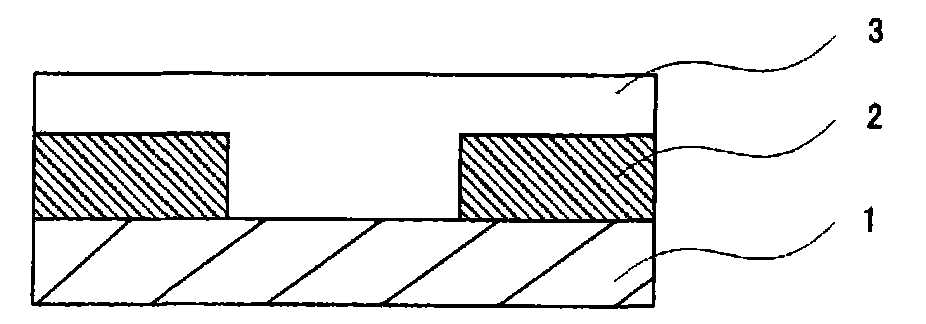
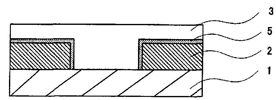
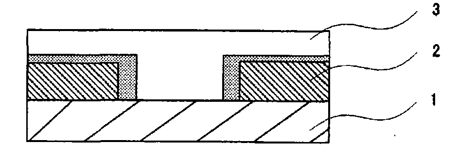
[0068] A KrF resist (DX5250P (registered trademark); manufactured by AZ Electronic Materials Co., Ltd.) was applied to a silicon wafer and subjected to exposure and development in usual methods to form a groove pattern of 1:3 or 1:5 pitch. Further, the fine pattern-forming composition prepared in Reference Example 1 was applied to the pattern. Then, the wafer was baked at 90° C. for 60 seconds. Subsequently, the baked pattern was rinsed with dibutyl ether for 60 seconds, and then centrifuged and dried to obtain the pattern. The amount of shrinkage was calculated by measuring the groove width of the pattern with a length measuring scanning microscope (critical dimension SEM S-9200, manufactured by Hitachi, Ltd.) before and after the treatment with the composition for fine pattern formation. The obtained results are shown in Table 1.
[0069] [Table 1]
[0070] Pattern type
[0071] These results show that the groove width was reduced by 16 nm by the treatment with ...
Embodiment 2
[0073] An ArF resist (AX1120P (registered trademark); manufactured by AZ Electronic Materials Co., Ltd.) was applied to a silicon wafer and subjected to exposure and development treatments by usual methods to form a groove pattern. Further, the fine pattern-forming composition prepared in Reference Example 1 was applied to the pattern. Then, the wafer was baked at 90° C. for 60 seconds. Subsequently, the baked pattern was rinsed with dibutyl ether for 60 seconds, and then centrifuged and dried to obtain the pattern. The amount of shrinkage was calculated by measuring the groove width of the pattern with a length measuring scanning microscope (S-9200, manufactured by Hitachi, Ltd.) before and after the treatment with the composition for fine pattern formation. The trench width was changed from 142nm to 127nm, which was confirmed to be reduced by 15nm.
PUM
 Abstract
Description
Claims
Application Information
 - R&D
- Intellectual Property
- Life Sciences
- Materials
- Tech Scout
- Unparalleled Data Quality
- Higher Quality Content
- 60% Fewer Hallucinations
Browse by: Latest US Patents, China's latest patents, Technical Efficacy Thesaurus, Application Domain, Technology Topic, Popular Technical Reports.
© 2025 PatSnap. All rights reserved.Legal|Privacy policy|Modern Slavery Act Transparency Statement|Sitemap|About US| Contact US: help@patsnap.com


