Inversion type encapsulation structure and manufacturing method thereof

A packaging structure, flip-chip technology, applied in semiconductor/solid-state device manufacturing, electrical components, electric solid-state devices, etc., can solve the problems of high heat generation of power devices, unfavorable heat dissipation of power devices, etc., to reduce the thermal resistance of packaging , shorten the process cycle, avoid the effect of leakage and crosstalk

Inactive Publication Date: 2010-06-30
SHANGHAI KAIHONG ELECTRONICS CO LTD
View PDF0 Cites 7 Cited by
  • Summary
  • Abstract
  • Description
  • Claims
  • Application Information

AI Technical Summary

Problems solved by technology

However, due to the high heat generation of power devices, an overly large package body is not conducive to the external heat dissipation of power devices during the packaging process.

Method used


Image

  • Inversion type encapsulation structure and manufacturing method thereof
  • Inversion type encapsulation structure and manufacturing method thereof
  • Inversion type encapsulation structure and manufacturing method thereof

Examples


Embodiment Construction

[0024] A specific implementation of a flip-chip packaging structure and a packaging method provided by the present invention will be described in detail below in conjunction with the accompanying drawings.

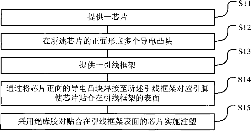
[0025] attached figure 1 Shown is a schematic diagram of the implementation steps of the method described in this specific embodiment, including: step S11, providing a chip; step S12, forming a plurality of conductive bumps on the front surface of the chip; step S13, providing a lead frame; step S14 , by welding the conductive bumps on the front of the chip to the corresponding pins of the lead frame, so that the chip is attached to the surface of the lead frame; step S15, using insulating glue to perform injection molding on the chip attached to the surface of the lead frame.

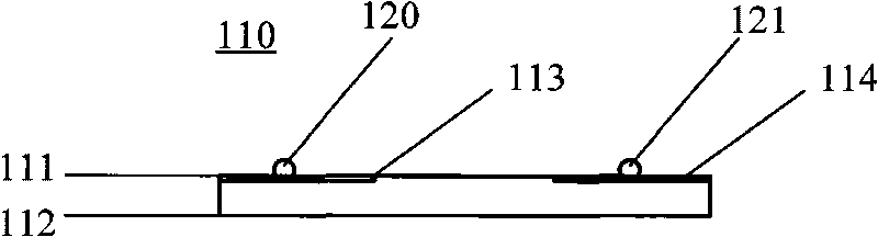
[0026] attached figure 2 to attach Figure 8 Shown is the process schematic diagram of above-mentioned method.

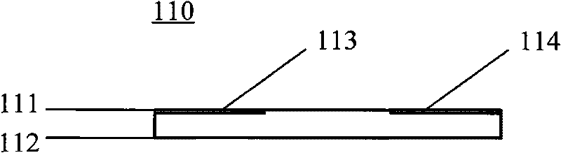
[0027] attached figure 2 As shown, referring to step S11, a chip 110 is provid...


PUM


Abstract

The invention relates to an inversion type encapsulation structure, comprising a lead wire frame which is provided with a plurality of lead feet; a chip which is arranged on the lead wire frame and is provided with a front surface and a back surface, and the front surface is provided with a plurality of bonding pads which are electrically connected to the lead feed corresponding to the lead wire frame; a plurality of conductive lugs which are arranged between the chip and the lead wire frame and are electrically connected with the bonding pads of the chip and the lead feet of the lead wire frame; and a plastic body which is arranged on the surface of the lead wire frame, wherein the chip is arranged; the inversion type encapsulation structure has the advantages that: by adopting the method that the conductive lugs are directly bonded the lead wire frame, the process period is shortened, the encapsulation resistance between the lead wire frame and the chip can be reduced; metal lines are replaced by the lugs, creepage and crosstalk among the lead wires and the effect of external electromagnetic radiation on the working of the chip are avoided; in the preferential technical proposal, the back surface of the chip is exposed to outside of the plastic body, the encapsulation heat resistance is reduced.

Description

【Technical field】 [0001] The invention relates to the field of chip packaging, in particular to a flip-chip packaging structure and a packaging method thereof. 【Background technique】 [0002] As the integration level of semiconductor integrated circuits is getting higher and higher, and the working speed is getting faster and faster, the heat dissipation requirements for chip packaging structures are also becoming more and more stringent. Especially for power devices, since they need to work in high-voltage, high-current or high-frequency environments, the requirements for the insulation characteristics of the chip packaging structure are very strict, and the chip volume of power devices is usually large, resulting in power The packaging structure obtained after the device is packaged in the prior art is bulky. However, since the power device generates a lot of heat, an overly large package body is not conducive to the external heat dissipation of the power device during th...

Claims


Application Information

Patent Timeline
Patent Type & Authority Applications(China)
IPC IPC(8): H01L23/485H01L23/495H01L23/31H01L21/50H01L21/60H01L21/56
CPCH01L2224/16245
Inventor 张江元柳丹娜李志宁
Owner SHANGHAI KAIHONG ELECTRONICS CO LTD
Why Eureka
Try Eureka