
Device for charging dry air or nitrogen gas into semiconductor wafer storage container and wafer static charge removing apparatus utilizing the device

A technology of dry air and storage containers, which is applied in semiconductor/solid-state device manufacturing, circuits, electrical components, etc., can solve the problems that cannot be completely solved, cannot completely prevent semiconductor wafer static electricity, dust flying, etc., and achieve the effect of preventing corrosion

Inactive Publication Date: 2010-06-09
KONDO IND +1
View PDF0 Cites 9 Cited by
  • Summary
  • Abstract
  • Description
  • Claims
  • Application Information

AI Technical Summary

Problems solved by technology

In addition, there is also a problem that due to the high-speed inflow of the above-mentioned initial dry air or nitrogen gas, the dust located on the bottom of the semiconductor wafer storage container or the back surface of the wafer will fly and adhere to the semiconductor circuit on the surface of the wafer.
[0007] In addition, a method of controlling the inflow velocity into the semiconductor wafer storage container with a mass flowmeter or the like has also been tried, but even if a mass flowmeter is installed, the fluctuation of the flow velocity at the start of inflow cannot be suppressed, and the mass flowmeter is extremely expensive. High, so there is a problem of huge investment
[0008] On the other hand, with the advancement of miniaturization of semiconductors, the particle size of dust in the manufacturing process has also become nanoscale, and weak static electricity will cause damage to circuits and adhesion of dust. The method of mixing conductive substances such as carbon cannot completely prevent the static electricity carried by the semiconductor wafer. On the contrary, if the amount of carbon is increased, it will also cause chemical gas from the semiconductor wafer storage container, which will not completely solve the problem related to the static electricity of the semiconductor wafer. The problem
[0009] In addition, when a semiconductor manufacturer stores a semiconductor wafer in a semiconductor wafer storage container, a method of blowing ionized air into the open opening and then closing the lid with the lid of the semiconductor wafer storage container opened has been tried, and there are also The problem with little effect

Method used


Image

  • Device for charging dry air or nitrogen gas into semiconductor wafer storage container and wafer static charge removing apparatus utilizing the device
  • Device for charging dry air or nitrogen gas into semiconductor wafer storage container and wafer static charge removing apparatus utilizing the device
  • Device for charging dry air or nitrogen gas into semiconductor wafer storage container and wafer static charge removing apparatus utilizing the device

Examples


Embodiment 1

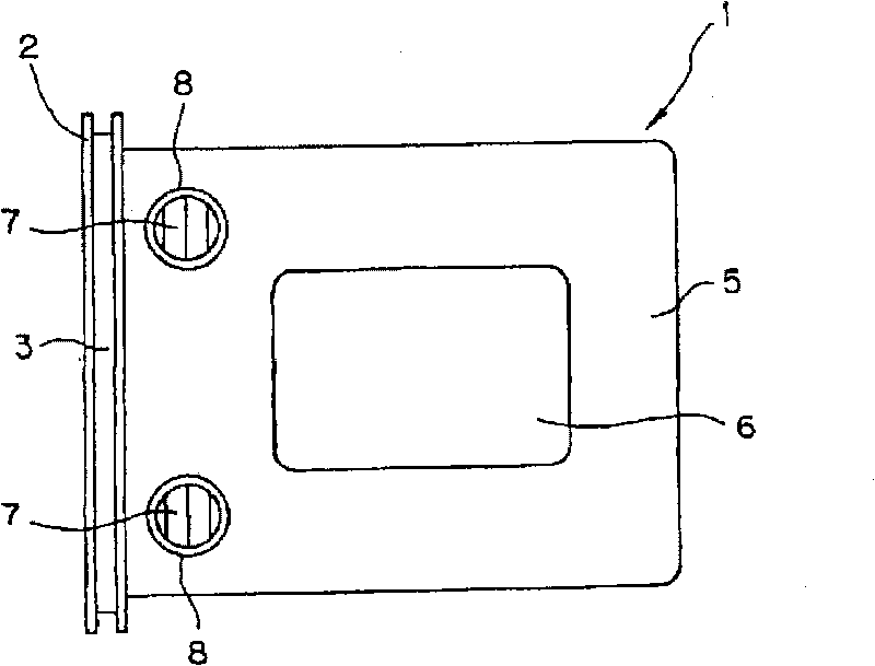
[0051] The filling device of dry air or nitrogen in Embodiment 1 of the present invention will be described in detail with reference to the drawings. figure 1 is a longitudinal sectional view of a semiconductor wafer storage container used in the present invention, figure 2 is the bottom view of the figure. Such as figure 1 , figure 2 As shown, on the semiconductor wafer storage container 1, an openable and closable cover 3 provided with a cover flange 2 is installed on the front surface, and a lifting hook 4 for lifting the semiconductor wafer storage container 1 is installed on the top, and furthermore, on the bottom plate Legs 6 for mounting on a not-shown mounting table or the like, and a plurality of breathing ports 8 provided with PTFE filters 7 are provided on 5 .

[0052] The semiconductor wafer 9 is accommodated in the above-mentioned semiconductor wafer storage container 1, and the semiconductor wafer 9 is processed by a process device (not shown). Adhesive che...

Embodiment 2

[0066] As a second embodiment of the present invention, a static eliminator using a filling device of dry air or nitrogen gas obtained by the above configuration will be described in detail with reference to the drawings.

[0067] Figure 8 It is a plan view of the static elimination device using the dry air or nitrogen filling device of the present invention, Figure 9 It means that the antistatic device is installed on the figure 1 , figure 2 A longitudinal cross-sectional view of the state of the semiconductor wafer storage container shown. Such as Figure 8 , Figure 9 As shown, the static eliminator B that removes the static electricity carried by the semiconductor wafer 9 in the semiconductor wafer storage container 1, the dry air / nitrogen supply unit 11 that supplies dry air or nitrogen in the above-mentioned dry air or nitrogen filling device A, Used as the ionized dry air / ionized nitrogen gas supply part 11a, and the used dry air or nitrogen gas discharge part 1...


PUM


Abstract

Without the need to open the lid of semiconductor wafer storage container, there can be attained removal of any chemical gas present in the semiconductor wafer storage container and inhibition of acid generation therein. There is provided dry air or nitrogen gas charging device (A) connected and fixed to supply-side respiration orifice (8a) and discharge-side respiration orifice (8b) among multiple respiration orifices (8) disposed in bottom board (5) of semiconductor wafer storage container (1) accommodating semiconductor wafers (9), each of the respiration orifices (8a,8b) equipped with PTFE filter (7), which charging device (A) comprisesdry air / nitrogen gas supply part (11) for supplying dry air or nitrogen gas into the semiconductor wafer storage container (1) and used dry air / nitrogen gas discharge part (12) for discharging the dry air or nitrogen gas after, by means of the dry air or nitrogen gas fed into the semiconductor wafer storage container (1), not only removal of chemical gas within the semiconductor wafer storage container (1) but also inhibition of acid generation on the surface of semiconductor wafers by moisture removal.

Description

technical field [0001] The present invention relates to a method for removing chemical gas and moisture in a semiconductor wafer storage container containing semiconductor wafers used in semiconductor manufacturing, preventing acid generation on the surface of the semiconductor wafer, and filling the semiconductor wafer storage container with dry air or A device for filling nitrogen gas and a static eliminator using this device to remove static electricity from the surface of a semiconductor wafer. Background technique [0002] Conventionally, in the semiconductor manufacturing process in the micro-environment type clean room, the processing process has become more and more complicated with the development of miniaturization of semiconductor wafers. In particular, in the etching process using halogen gas, the residual halogen gas after etching reacts with moisture in dry air to generate acid, and the corrosion of semiconductor wafers caused by this acid will become a major p...

Claims


Application Information

Patent Timeline
Patent Type & Authority Applications(China)
IPC IPC(8): H01L21/673
CPCH01L21/68H01L21/67396H01L21/67017H01L21/67393
Inventor 木崎原稔郎冈田诚饭田尚司本田康
Owner KONDO IND
Learn More