
Lug structure and making method thereof

A technology of bumps and elastic layers, applied in semiconductor/solid-state device manufacturing, electrical components, electric solid-state devices, etc.

Inactive Publication Date: 2010-06-09
HANNSTAR DISPLAY CORPORATION
View PDF0 Cites 2 Cited by
  • Summary
  • Abstract
  • Description
  • Claims
  • Application Information

AI Technical Summary

Problems solved by technology

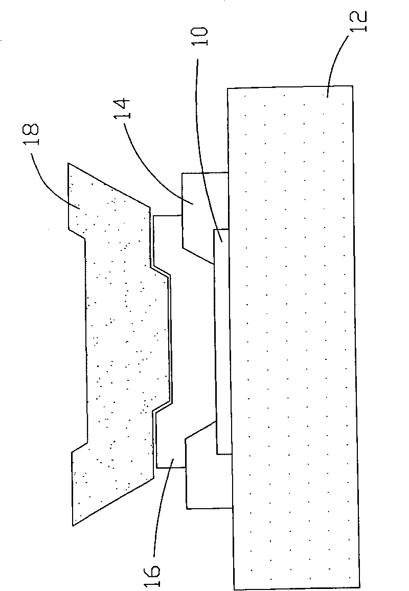
Generally speaking, the pitch of finepitch IC bumps is usually lower than 20 μm, and the limit value of the distance between the exposure and development capabilities of the PI layer material is 20 μm. Under such a spacing limit, the pitch will be a (a < 20 μm) The island-shaped elastic layer faces a major bottleneck in the production

Method used


Image

  • Lug structure and making method thereof
  • Lug structure and making method thereof
  • Lug structure and making method thereof

Examples


Embodiment Construction

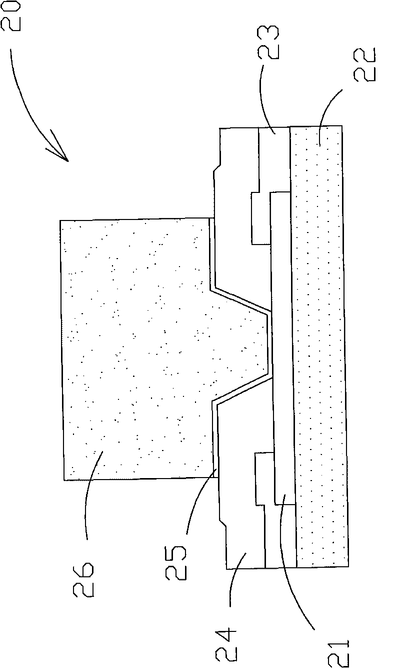
[0041] The main spirit of the smart bump structure of the first embodiment of the present invention is based on the smart structure design of the prior art. In order to cope with the continuous development of ICs with fine pitches, the pitch of IC bumps with fine pitches needs to be lower than 20μm, and the development and etching limit of the elastic layer spacing is 20μm, providing a new smart bump structure allows the bumping house to have more margins and successfully form a smart bump structure.

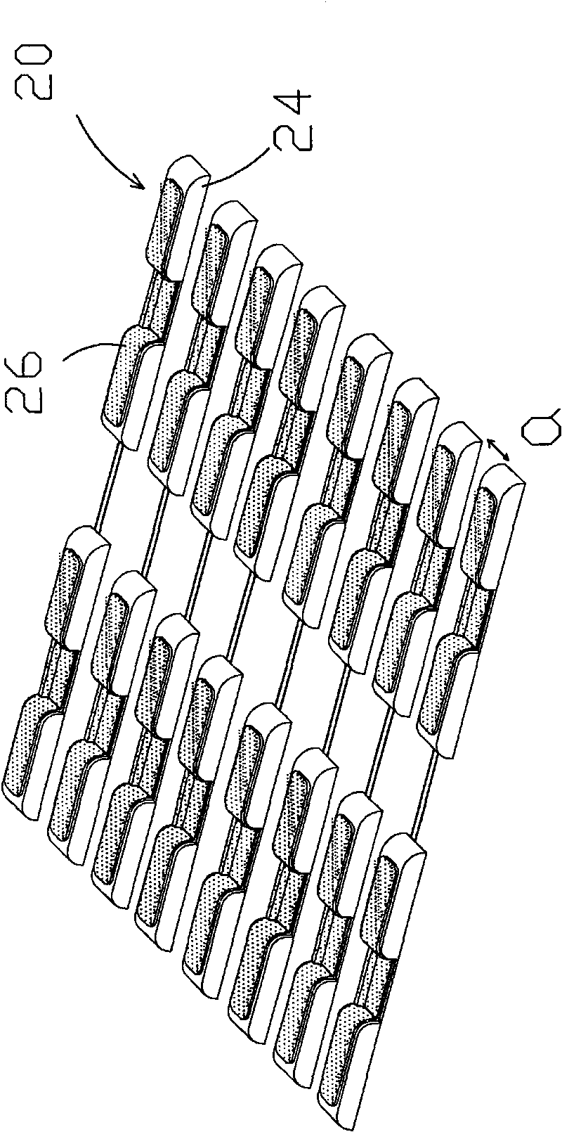
[0042] Please also refer to Figure 3(a) ~ Figure 3(c) , which is a schematic perspective view of the first embodiment of the present invention, a cross-sectional view of section line bb' and a schematic layout of the structure. The main technical difference between this embodiment and the existing smart bump is that a patterned elastic layer of the present invention bears at least two bump structures.

[0043]As shown in the figure, the structure of the smart bump 30 of the pr...


PUM


Abstract

The invention relates to a lug structure and a making method thereof. The lug structure comprises a semiconductor substrate, a protective layer, an elastic layer and a plurality of lugs, wherein a plurality of connection pads are formed on the surface of the semiconductor substrate; the protective layer is covered on the substrate and provided with openings corresponding to the connection pads, thereby exposing part of each connection pad as the electric connection position; the elastic layer is positioned on the protective layer; and each lug is positioned on the electric connection position and extends to the elastic layer, thereby providing the space between the lug elasticity and the amount of deformation by means of the elastic layer. In the invention, a large-size (at least 20 mu m) elastic layer pattern making procedure is utilized to form the elastic layer with a proper pattern, so that the lug structure can be suitable for IC elements with superfine pitch.

Description

【Technical field】 [0001] The invention relates to a metal bump structure and a manufacturing method thereof, in particular to a bump structure and a manufacturing method thereof. 【Background technique】 [0002] The liquid crystal display (Liquid Crystal display, LCD) process includes three stages of process, such as array (array), unit cell (cell) and module (module). The block process is divided into three parts, which are COG (chip on glass), OLB (outer lead bonding) and AOP (ACF on PCB). Among the three LCM (LCD Module) manufacturing processes, the COG module assembly technology has the advantages of high joint density and low cost, and is designed as a key point to reduce costs. The so-called Chip on Glass (COG) is a high pin count (high pin count) and super fine pitch (fine pitch) flat panel display (Flat Panel Display) module construction technology. The technical feature of this module assembly is that there are minimum joints between the driver IC signal source and...

Claims


Application Information

Patent Timeline
IPC IPC(8): H01L23/485H01L21/60
Inventor 孙伟豪汤宝云
Owner HANNSTAR DISPLAY CORPORATION
Learn More