Image sensor and method of fabricating the same

An image sensor and pattern technology, applied in semiconductor/solid-state device manufacturing, electrical solid-state devices, semiconductor devices, etc., can solve problems such as increased leakage current, inability to form contacts well, and damage

Inactive Publication Date: 2010-06-09
DONGBU HITEK CO LTD
View PDF12 Cites 1 Cited by
  • Summary
  • Abstract
  • Description
  • Claims
  • Application Information

AI Technical Summary

Problems solved by technology

When the etching depth is increased to ensure the etching margin to form a contact hole in the logic area, the etching depth of the contact hole in the pixel area increases, so that the photodiode, especially, the floating diffusion area is damaged, so Leakage current increases and dark current characteristics deteriorate
[0008] On the other hand, when reducing the etch allowance of the contact hole in the logic area to prevent damage to the pixel area due to etching, the contacts in the logic area composed of many circuits cannot be well formed.

Method used


Image

  • Image sensor and method of fabricating the same
  • Image sensor and method of fabricating the same
  • Image sensor and method of fabricating the same

Examples


Embodiment Construction

[0019] Hereinafter, technical concerns matters and features of the present invention will be clearly understood through the description of the accompanying drawings and embodiments. Preferred embodiments of the present invention will be described below.

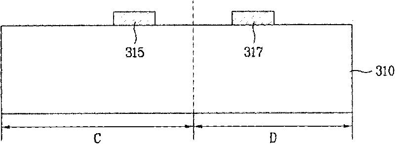
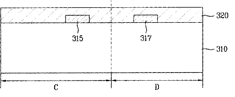
[0020] 2A to 2F are longitudinal sectional views illustrating a method of manufacturing an image sensor according to one embodiment of the present invention.

[0021] First, as shown in FIG. 2A, a substrate (for example, a silicon substrate) 310 on which a pixel region C and a logic region D are defined is prepared. A unit pixel for detecting light is formed on a substrate in the pixel region C, and a logic circuit is formed in the logic region D, wherein the logic circuit includes at least one transistor for processing the light detected by the pixel region C into Electrical signals to obtain optical data.

[0022] At least one transistor is formed on the substrate in each of the pixel region C and the logic region D. FIG...


PUM


Abstract

A method of fabricating an image sensor, including: preparing a substrate including a pixel region and a logic region respectively having transistors, wherein the transistors comprise gates formed on a pixel region a logic region; forming a first interlayer dielectric film on a substrate to cover gates; first contact holes exposing a region of a substrate and a part of a gate on a pixel region by selectively etching a first interlayer dielectric film formed on a pixel region; forming first contacts by filing the first contact holes with a metal material; forming a second interlayer dielectric film on the entire surface of the first interlayer dielectric film; simultaneously forming second contact holes which may penetrate a second interlayer dielectric film on a pixel region to expose first contacts, and forming third contact holes which may penetrate a second interlayer dielectric film and the first interlayer dielectric film on the logic region to expose a part of a gate and a region of a substrate on the logic region; and forming second contacts by filling second contact holes and third contact holes with the metal material.

Description

[0001] This application claims priority from Korean Patent Application No. 10-2008-0104139 filed on October 23, 2008, the entire contents of which are hereby incorporated by reference. technical field [0002] The present invention relates to a semiconductor device, and more particularly, to a method of manufacturing a CMOS image sensor. Background technique [0003] Image sensors refer to semiconductor devices that convert optical images into electrical signals. Image sensors are classified into charge coupled device (Charge Coupled Device, CCD) image sensors and complementary metal oxide silicon (Complementary Metal-Oxide-Silicon, CMOS) image sensors. [0004] The image sensor includes a pixel area including a photodiode for detecting light and a logic area for processing the detected light into an electrical signal to obtain optical data. That is, the image sensor may refer to a device that receives light incident to a pixel region and captures an image using a photodiod...

Claims


Application Information

Patent Timeline
Patent Type & Authority Applications(China)
IPC IPC(8): H01L21/82H01L21/768H01L27/146
CPCH01L27/14636H01L27/14603H01L27/14689H01L27/146
Inventor 张勋
Owner DONGBU HITEK CO LTD
Why Eureka
Try Eureka