Silicon-based filed emission cathode material with low threshold electric field and preparation method thereof
A field emission cathode and emission cathode technology, which is applied in cold cathode manufacturing, electrode system manufacturing, discharge tube/lamp manufacturing, etc., can solve the problems of complex emission cathode preparation process, low emission current density, and poor emission stability, etc. Great commercial application potential, simple and easy fabrication process, and the effect of high emission current density
- Summary
- Abstract
- Description
- Claims
- Application Information
AI Technical Summary
Problems solved by technology
Method used
Image
Examples
Embodiment 1
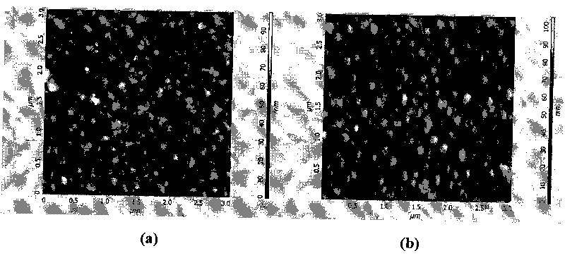
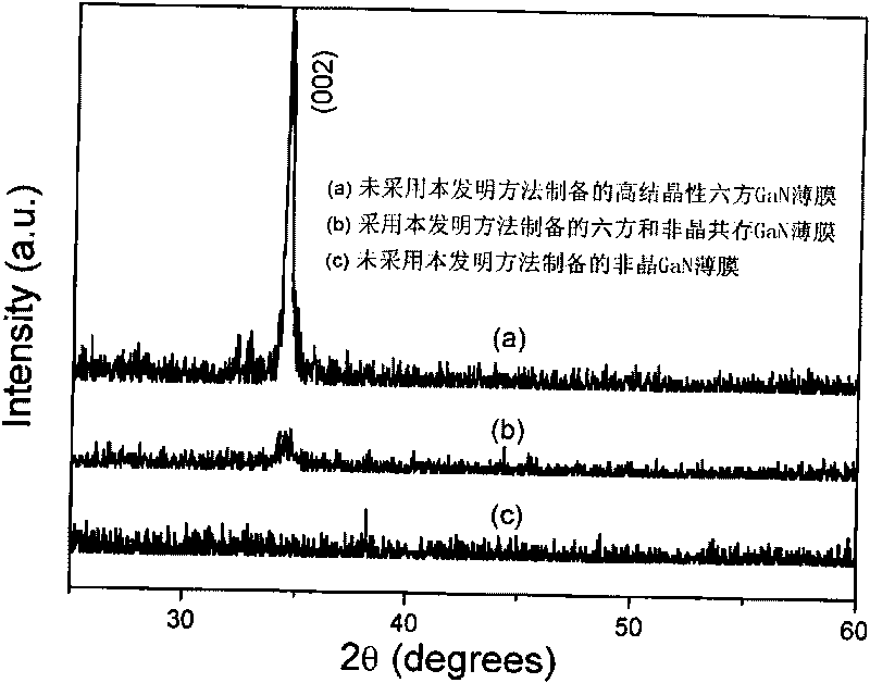
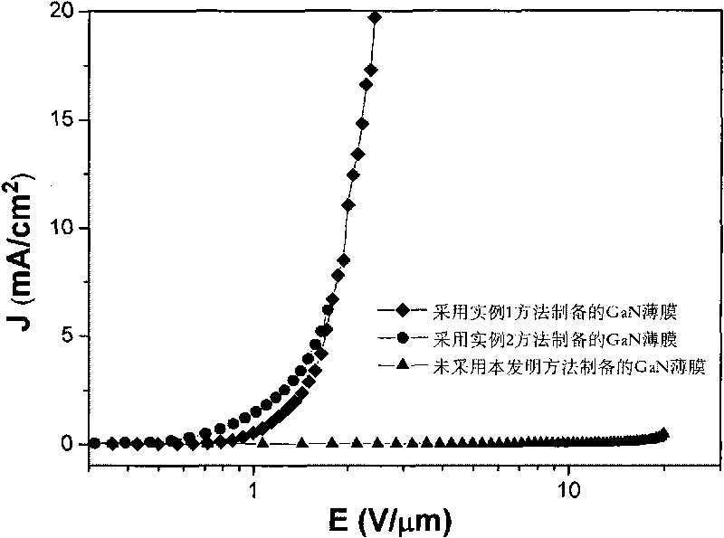
[0037] The polished n-type (100) silicon was soaked in HF acid with a volume concentration of 3% for 2 minutes as the substrate, and the gallium nitride powder with a purity of 99.99% was sintered at 560°C for 120 minutes to make a gallium nitride target, and the substrate and target were placed in In the cavity of the laser pulse deposition system, the deposition chamber is pumped to about 5×10 -4 Pa, and heat the silicon substrate to 850°C, supply nitrogen with a purity of 99.99% as a protective gas and adjust the working pressure of the deposition chamber to 1Pa, set the frequency of the pulse laser to 13Hz, and start to deposit hexagonal ( 002) The gallium nitride thin film with preferred orientation and amorphous phase coexists, and the average thickness of the thin film reaches 40nm after maintaining for 2 minutes. The field emission current density is 1mA / cm 2 , the required applied electric field strength is 1.2V / μm.
Embodiment 2
[0039] The polished n-type (100) silicon was soaked in HF acid with a volume concentration of 3% for 2 minutes as the substrate, and the gallium nitride powder with a purity of 99.99% was sintered at 560°C for 120 minutes to make a gallium nitride target, and the substrate and target were placed in In the cavity of the laser pulse deposition system, the deposition chamber is pumped to about 5×10 -4Pa, and heat the silicon substrate to 850°C, supply nitrogen with a purity of 99.99% as a protective gas and adjust the working pressure of the deposition chamber to 1Pa, set the frequency of the pulse laser to 13Hz, and start to deposit hexagonal ( 002) GaN thin film with preferred orientation and amorphous phase coexistence, maintain the time for 1.5min to make the average thickness of the thin film reach 30nm. The field emission current density is 1mA / cm 2 , the required applied electric field strength is 0.9V / μm.
Embodiment 3
[0041] The polished n-type (100) silicon was soaked in HF acid with a volume concentration of 3% for 2 minutes as the substrate, and the aluminum nitride powder with a purity of 98% was sintered at 560°C for 120 minutes to make an aluminum nitride target, and the substrate and target were placed in In the cavity of the laser pulse deposition system, the deposition chamber is pumped to about 1×10 -4 Pa, and heat the silicon substrate to 900°C, supply nitrogen with a purity of 99.99% as a protective gas and adjust the working pressure of the deposition chamber to 0.5Pa, set the frequency of the pulse laser to 12Hz, and the pulse energy to 350mJ / pulse and start to deposit hexagonal (002) AlN thin film with preferred orientation and amorphous phase coexistence, maintain the time for 1.5min to make the average thickness of the film reach 25nm. The field emission current density is 1mA / cm 2 , the required applied electric field strength is 2.1V / μm.
PUM
| Property | Measurement | Unit |
|---|---|---|
| thickness | aaaaa | aaaaa |
| thickness | aaaaa | aaaaa |
Abstract
Description
Claims
Application Information
 - R&D
- Intellectual Property
- Life Sciences
- Materials
- Tech Scout
- Unparalleled Data Quality
- Higher Quality Content
- 60% Fewer Hallucinations
Browse by: Latest US Patents, China's latest patents, Technical Efficacy Thesaurus, Application Domain, Technology Topic, Popular Technical Reports.
© 2025 PatSnap. All rights reserved.Legal|Privacy policy|Modern Slavery Act Transparency Statement|Sitemap|About US| Contact US: help@patsnap.com


