Solid-state image sensor and camera system

A solid-state image and sensor technology, which is applied in the field of camera systems, can solve problems such as noise generation, and achieve the effects of suppressing the increase in circuit area, reducing AD converter noise, and increasing frame rate

Active Publication Date: 2010-06-02
SONY CORP
View PDF3 Cites 25 Cited by
  • Summary
  • Abstract
  • Description
  • Claims
  • Application Information

AI Technical Summary

Problems solved by technology

However, noise does occur when resetting the last sampled capacitor voltage level to some reference value

Method used


Image

  • Solid-state image sensor and camera system
  • Solid-state image sensor and camera system
  • Solid-state image sensor and camera system

Examples


Embodiment Construction

[0037] Embodiments of the present invention will be described below with reference to the accompanying drawings. It will be described as follows.

[0038] 1. Overall example structure of solid-state image sensor

[0039] 2. Example structure of comparator

[0040] 3. CDS considerations

[0041] 4. Comparator operation

[0042] 5. Modification example of comparator

[0043] 6. Example structure of camera system

[0044]

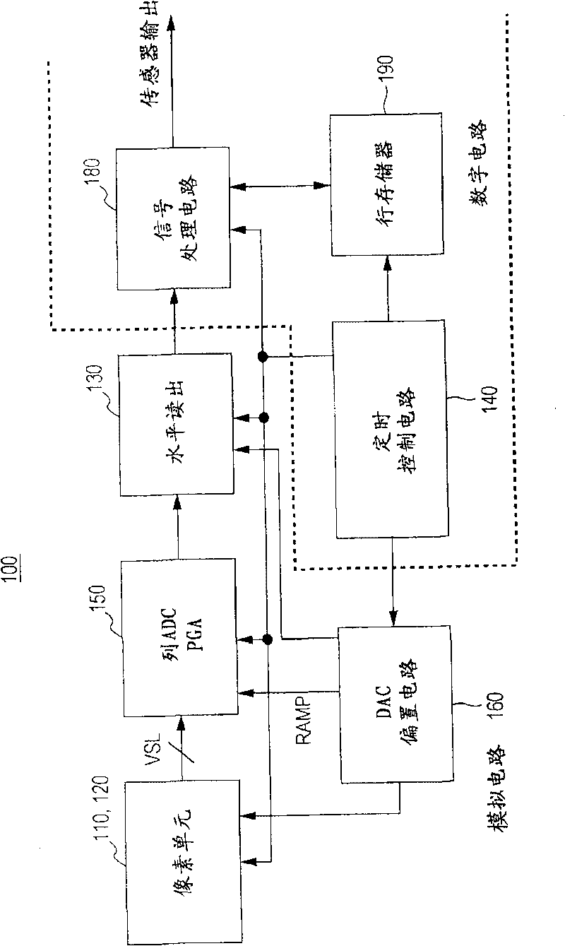
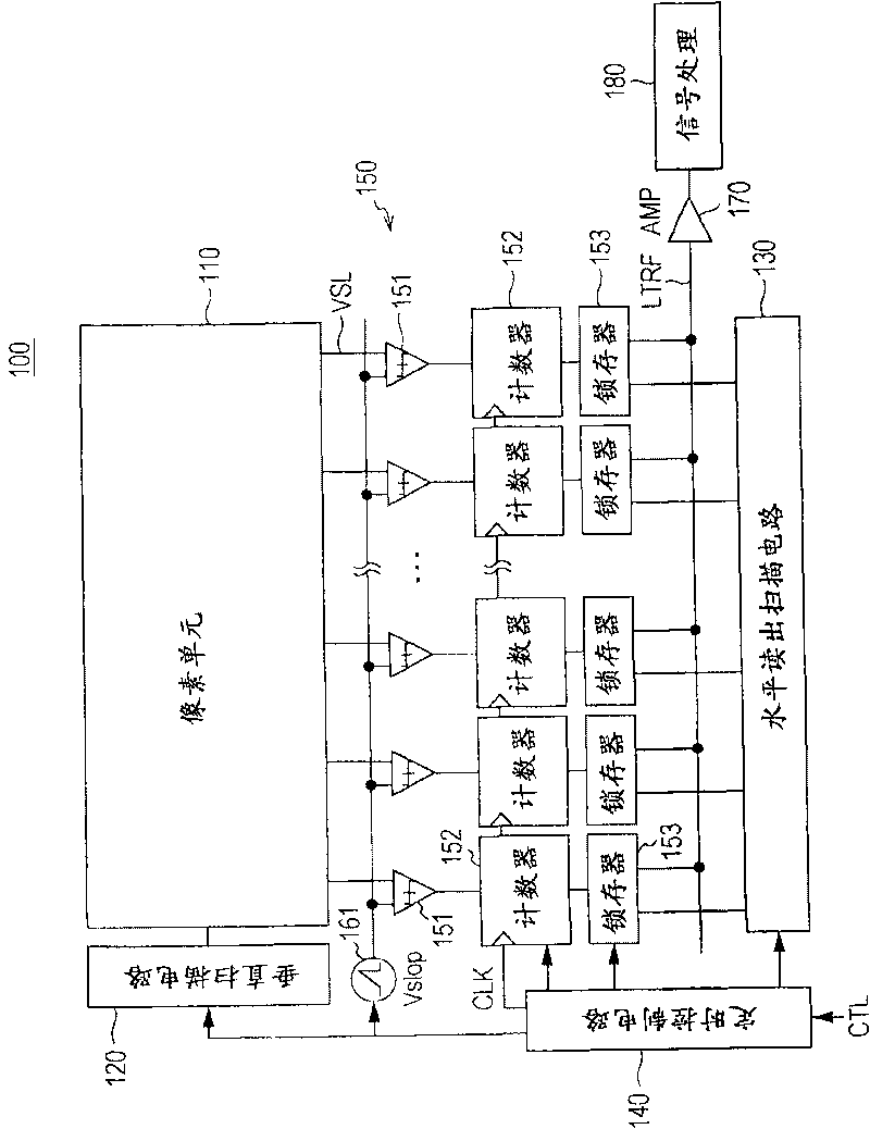
[0045] figure 1 is a block diagram illustrating an example structure of a column-parallel ADC solid-state image sensor (ie, a CMOS image sensor) according to an embodiment of the present invention. figure 2 is a more detailed explanation figure 1 A block diagram of an ADC bank in a column-parallel ADC solid-state image sensor (ie, a CMOS image sensor) is shown.

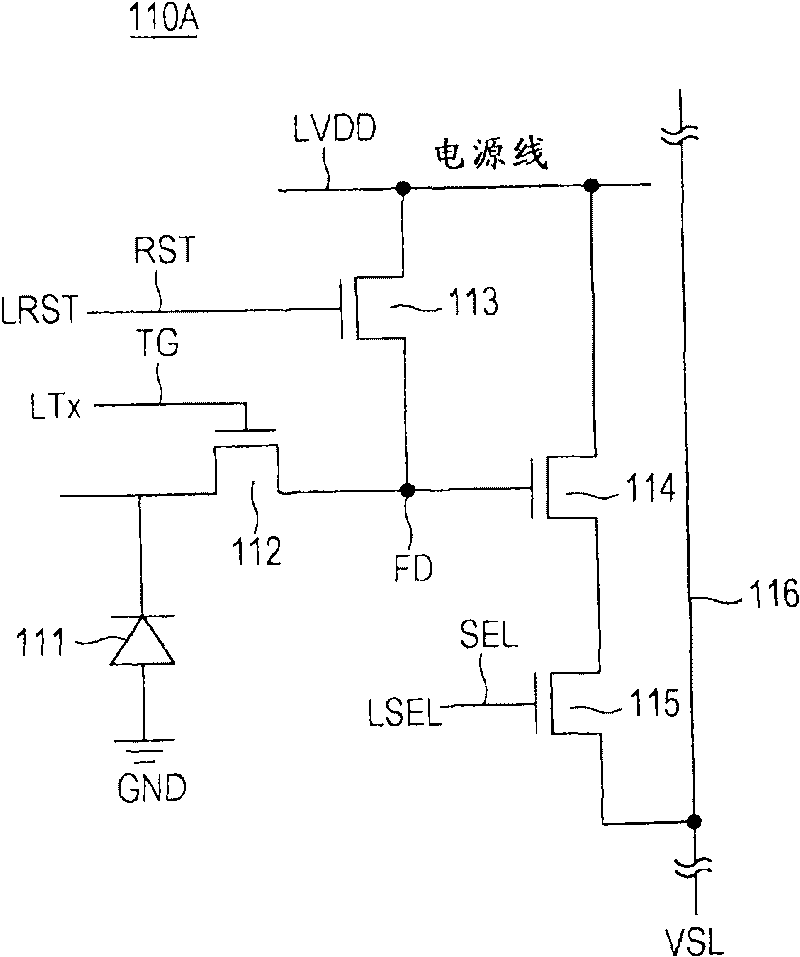
[0046] like figure 1 and 2 As shown, the solid-state image sensor 100 includes a pixel unit 110 constituting an imaging module, a vertical scanning circuit 120 , a horizontal readout scanni...


PUM


Abstract

A solid state image sensor includes a pixel unit and a readout unit that reads out per-pixel pixel signals from the pixel unit. The readout unit includes: a plurality of column-parallel comparators that compare a readout signal potential to a reference voltage and output a determination signal; and a plurality of counters that count the comparing time of a corresponding comparator. Each comparator includes: a first amp containing a differential amplifier that receives the reference voltage at the gate of a transistor, receives the readout signal at the gate of another transistor, and compares the reference voltage to the readout signal potential; a second amp containing an amplifier that increases the gain of the first amp's output; and a capacitor connected between the input and the output of the amplifier in the second amp in order to exhibit the Miller effect.

Description

technical field [0001] The present invention relates to solid state image sensors, typically CMOS image sensors, and camera systems. Background technique [0002] In recent years, CMOS image sensors have attracted attention in replacing CCDs as solid-state image sensors. This focus is due to the following reasons. The fabrication of CCD pixels involves dedicated processing, and their operation involves multiple supply voltages. In addition, CCDs need to work together with multiple peripheral ICs. In contrast, CMOS image sensors overcome several problems associated with the significantly increased system complexity of such CCDs. [0003] The CMOS image sensor can be fabricated using a fabrication process similar to that of a typical CMOS integrated circuit. It is also possible to drive a CMOS image sensor using a single power supply. In addition, CMOS image sensors can be mixed together with analog or logic circuits on a single chip using a CMOS process. For these reaso...

Claims


Application Information

Patent Timeline
Patent Type & Authority Applications(China)
IPC IPC(8): H04N5/335H04N3/15H04N5/225H04N5/357H04N5/363H04N5/369H04N5/374H04N5/378
CPCH04N5/3575H03F3/08H04N5/378H04N25/616H04N25/75H04N25/60H04N25/76
Inventor 蓟纯一郎
Owner SONY CORP
Why Eureka
Try Eureka