Substrate placing stage and substrate processing apparatus

A technology for mounting table and substrate, applied in optics, instruments, discharge tubes, etc., can solve the problems of different etching rates and uneven electromagnetic fields, and achieve the effect of eliminating uneven electromagnetic fields, reducing the number and reducing work.

Active Publication Date: 2010-05-12
TOKYO ELECTRON LTD
View PDF1 Cites 16 Cited by
  • Summary
  • Abstract
  • Description
  • Claims
  • Application Information

AI Technical Summary

Problems solved by technology

[0007] However, in the case of performing plasma processing such as plasma etching on an insulating substrate such as a glass substrate or a quartz substrate, the sheath (sheath) region will The electromagnetic field is not uniform, so it is clear that the etching rate of the position directly above the hole of the lift pin is different from that of other parts

Method used


Image

  • Substrate placing stage and substrate processing apparatus
  • Substrate placing stage and substrate processing apparatus
  • Substrate placing stage and substrate processing apparatus

Examples


Embodiment Construction

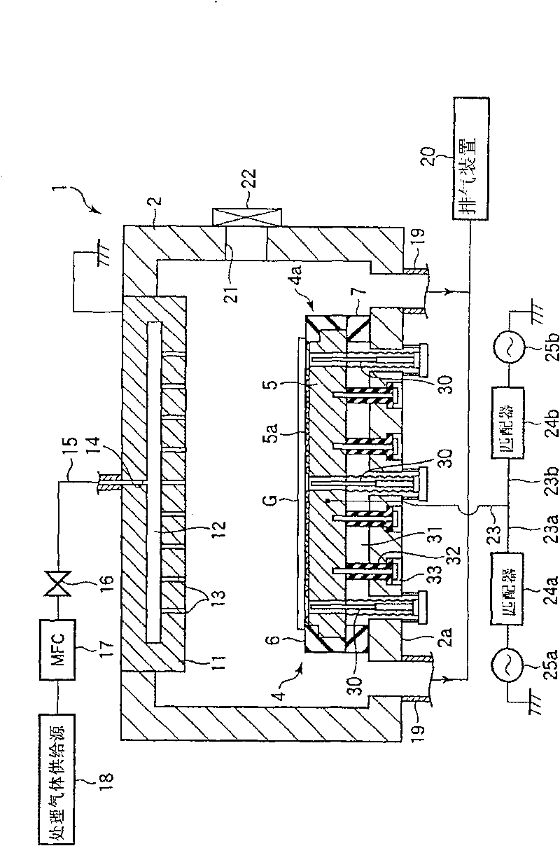
[0045] Embodiments of the present invention will be described below with reference to the drawings. figure 1It is a cross-sectional view showing a plasma etching apparatus as an example of a processing apparatus provided with a susceptor as a substrate mounting table according to an embodiment of the present invention. This plasma etching apparatus 1 performs predetermined processing on a glass substrate G for FPD The cross-sectional view of the device is configured as a capacitively coupled parallel plate plasma etching device. Here, examples of the FPD include a liquid crystal display (LCD), a light emitting diode (LED) display, an electroluminescence (Electro Luminescence; EL) display, Fluorescent display tube (Vacuum Fluorescent Display; VFD), plasma display panel (PDP), etc.

[0046] The plasma etching apparatus 1 has a square cylinder-shaped chamber 2 made of, for example, aluminum whose surface is treated with an aluminum oxide film (anodized treatment).

[0047] A sus...


PUM


Abstract

The present invention provides a substrate placing stage (4) which is hard to cause an evenness in process at the position corresponding to an insert hole of a lifting pin of a placing stage body when the substrate (G) is subjected to plasma process. In the plasma process the substrate placing stage (G) for placing the substrate (4) is arranged in a processing container (2) by a partition (7) composed of an insulating component, which forms a space (31) between the substrate placing stage (G) and the bottom wall (2a) of the processing container (2), and the space (31) is in an air atmosphere.

Description

technical field [0001] The present invention relates to a substrate mounting table for placing a substrate in a processing container in a substrate processing apparatus for dry etching a substrate such as a glass substrate or a semiconductor wafer for manufacturing a flat panel display (FPD) such as a liquid crystal display device (LCD), and A substrate processing apparatus using the substrate mounting table. Background technique [0002] For example, in the manufacturing process of FPDs and semiconductors, various treatments such as dry etching, sputtering, and CVD (Chemical Vapor Growth) are performed on glass substrates or semiconductor wafers as substrates to be processed. [0003] Such processing is performed, for example, with the substrate placed on a substrate mounting table provided in the chamber. The loading and unloading of the substrate on the substrate stage is performed by raising and lowering a plurality of lift pins included in the substrate stage. That is...

Claims


Application Information

Patent Timeline
Patent Type & Authority Applications(China)
IPC IPC(8): H01L21/683H01L21/00
CPCG02F1/1303H01J37/32082H01J37/3244H01J37/32532H01J37/32715H01L21/67017H01L21/68742H01L21/68785
Inventor 天野健次田中善嗣
Owner TOKYO ELECTRON LTD
Why Eureka
Try Eureka