
Mixed crystal orientation strain silicon substrate and method for preparing same

A technology of mixed crystal orientation and strained silicon, which is used in semiconductor/solid-state device manufacturing, electrical components, electrical solid-state devices, etc. The effect of reducing the dislocation density and avoiding the relaxation of the lattice

Inactive Publication Date: 2012-05-23
SHANGHAI SIMGUI TECH +1
View PDF0 Cites 0 Cited by
  • Summary
  • Abstract
  • Description
  • Claims
  • Application Information

AI Technical Summary

Problems solved by technology

[0004] The problem of the prior art is that the substrate with mixed crystal orientation has two or more different crystal orientations on the same substrate, and the dislocation density generated due to the stress mismatch of the crystal lattice is high, which cannot meet the requirements of Device application

Method used


Image

  • Mixed crystal orientation strain silicon substrate and method for preparing same
  • Mixed crystal orientation strain silicon substrate and method for preparing same
  • Mixed crystal orientation strain silicon substrate and method for preparing same

Examples


Embodiment Construction

[0020] The specific implementation of the mixed crystal direction strained silicon substrate and its preparation method provided by the present invention will be described in detail below with reference to the accompanying drawings.

[0021] Firstly, the specific implementation manner of the mixed crystal orientation strained silicon substrate of the invention will be given with reference to the accompanying drawings.

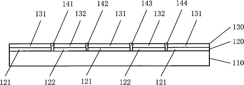
[0022] attached figure 1 Shown is a schematic structural diagram of the hybrid orientation strained silicon substrate in this specific embodiment, including: a support substrate 110 , a silicon germanium layer 120 , a strained silicon layer 130 and isolation grooves 141 - 144 .

[0023] The supporting substrate has a first crystal orientation.

[0024] The SiGe layer 120 is directly disposed on the surface of the supporting substrate, including a first SiGe region 121 and a second SiGe region 122 . The first SiGe region 121 has a first crystal orientation, an...


PUM

PropertyMeasurementUnit
thicknessaaaaaaaaaa
widthaaaaaaaaaa

Abstract

The invention provides a mixed crystal orientation strain silicon substrate, which comprises a support substrate, a germanium-silicon layer directly arranged on the surface of the support substrate and a strain silicon layer directly arranged on the surface of the germanium-silicon layer. The invention further provides a method for preparing the mixed crystal orientation strain silicon substrate.The mixed crystal orientation strain silicon substrate has the advantages of lowering dislocation density of the first germanium-silicon layer, ensuring the strain state of a first strain area, and improving quality of crystal lattice and strain degree of the strain silicon layer when used in the mixed crystal orientation strain silicon substrate as a buffer layer between the support substrate and the strain silicon layer. The preparation method has the advantages of not needing processes of polishing, epitaxy, linkage and the like after the strain silicon layer is fully developed and ensuring the strain degree of the strain silicon.

Description

【Technical field】 [0001] The invention relates to the field of semiconductor manufacturing, in particular to a mixed crystal orientation strained silicon substrate and a preparation method thereof. 【Background technique】 [0002] In the current semiconductor technology, CMOS circuits are mainly fabricated on silicon substrates with (100) crystal planes, because of the small oxide-interface charge density and the highest electron mobility on the (100) crystal planes . However, the mobility of holes is only about 1 / 4-1 / 2 of the corresponding electron mobility on (100) wafers, which makes the drive current of pMOSFETs prepared on (100) wafers about half that of nMOSFETs, While traditionally larger pMOSFETs can be used to balance nMOSFETs, in practice this increases gate and parasitic capacitance. It has been reported that the performance of pFETs can be improved by shifting the channel orientation from <110> to <100> on (100) substrates, but more work has focused ...

Claims


Application Information

Patent Timeline
Patent Type & Authority Patents(China)
IPC IPC(8): H01L23/00H01L29/04H01L21/02H01L21/20
CPCH01L2924/0002
Inventor 魏星王湘李显元张苗王曦林成鲁
Owner SHANGHAI SIMGUI TECH
Learn More