Organic el display panel and manufacturing method thereof
A luminescence and display technology, applied in the manufacture/processing of organic semiconductor devices, semiconductor/solid-state device manufacturing, circuits, etc., can solve problems such as fluctuations become more obvious, achieve uniform film thickness, high wettability, The effect of flattening the coated area
- Summary
- Abstract
- Description
- Claims
- Application Information
AI Technical Summary
Problems solved by technology
Method used
Image
Examples
Embodiment approach 1
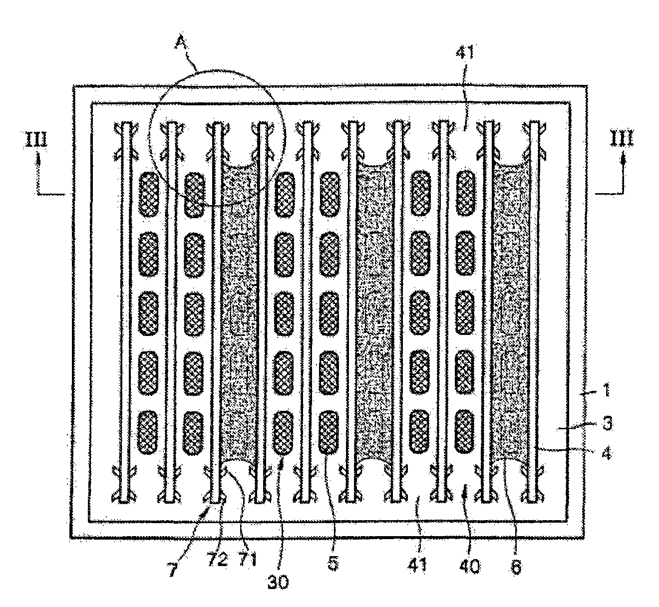
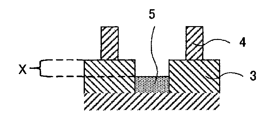
[0153] When the lower layer of the organic layer is a hole transport layer made of an oxide of a transition metal, the height of the second bank from the surface of the hole transport layer made of an oxide of a transition metal is preferably -0.1 to +0.4 μm, more preferably about 0 μm. In this way, when the lower layer of the organic layer is a hole transport layer made of transition metal oxide, the second bank does not need to define a layer formed by coating, so the second bank can be formed from the transition metal. The surface height of the hole transport layer made of oxide is low. Thereby, the inside of the application area can be made flat, and the film thickness of the organic layer can be made more uniform.
[0154] iii) When the lower layer of the organic layer is a hole transport layer containing PEDOT-PSS (see Embodiment 2)
[0155] When the lower layer of the organic layer is a hole transport layer made of a transition metal oxide, the height of the second ba...
Embodiment approach 2
[0213] In Embodiment 1, an example in which the hole transport layer is made of a transition metal oxide has been described. In Embodiment 2, an example in which the hole transport layer contains PEDOT-PSS will be described.
[0214] The organic EL display panel of Embodiment 2 is the same as the organic EL display panel of Embodiment 1 except that 1) the material of the hole transport layer is PEDOT-PSS and 2) the positional relationship between the second bank and the hole transport layer is different. Therefore, the same reference numerals are assigned to the same components as those in Embodiment 1, and description thereof will be omitted.
[0215] Figure 6A It is a plan view of an active matrix organic EL display panel according to Embodiment 2 omitting a counter electrode and an organic light-emitting layer. Figure 6B yes Figure 6A A perspective view of the organic EL display shown.
[0216] Figure 8A It is an A-A sectional view of the organic EL element include...
Embodiment approach 3
[0250] In Embodiments 1 and 2, an example in which the end portion in the longitudinal direction of the application region is not defined was described. In this embodiment, an example will be described in which the ends in the longitudinal direction of the application region are also defined by the first banks. In addition, in Embodiments 1 and 2, the method of disposing the second bank between the pixel region and the first bank was described (see FIG. 6 ), but in Embodiment 3, the description is made of A mode in which no second dike is arranged between one dike.
[0251] The organic EL display panel of the present embodiment is the same as the embodiment except that it has the first bank 105 ′ defining the end of the coating region and does not have the second bank 107 between the pixel region 120 and the first bank 105 . 1's organic EL display is the same. Therefore, the same reference numerals are assigned to the same components as those of the organic EL display panel ...
PUM
 Abstract
Description
Claims
Application Information
 - R&D Engineer
- R&D Manager
- IP Professional
- Industry Leading Data Capabilities
- Powerful AI technology
- Patent DNA Extraction
Browse by: Latest US Patents, China's latest patents, Technical Efficacy Thesaurus, Application Domain, Technology Topic, Popular Technical Reports.
© 2024 PatSnap. All rights reserved.Legal|Privacy policy|Modern Slavery Act Transparency Statement|Sitemap|About US| Contact US: help@patsnap.com


