
Oxide semiconductor electrode, dye-sensitized solar cell, and, method of producing the same

A technology of oxide semiconductor and manufacturing method, applied in semiconductor/solid-state device manufacturing, semiconductor device, capacitor electrode and other directions, can solve the problems of poor practicability, low energy conversion efficiency, and difficulty in dye-sensitized solar cells, etc. To achieve the effect of excellent stability over time and strong adhesion

Inactive Publication Date: 2010-03-10
DAI NIPPON PRINTING CO LTD
View PDF14 Cites 4 Cited by
  • Summary
  • Abstract
  • Description
  • Claims
  • Application Information

AI Technical Summary

Problems solved by technology

Due to this problem, it is difficult to manufacture dye-sensitized solar cells with excellent temporal stability using the transfer printing method
In addition, although the transfer method has the advantage of not having to consider the material of the substrate to be transferred, when the porous layer is transferred to the substrate to be transferred, there is still a fundamental problem that the porous layer is damaged. problem, thus having a problem of poor practicality
[0010] In addition, in general, since the energy conversion efficiency of dye-sensitized solar cells is lower than that of silicon solar cells, etc., an oxide semiconductor capable of further improving the energy conversion efficiency of dye-sensitized solar cells is required. electrode

Method used


Image

  • Oxide semiconductor electrode, dye-sensitized solar cell, and, method of producing the same
  • Oxide semiconductor electrode, dye-sensitized solar cell, and, method of producing the same
  • Oxide semiconductor electrode, dye-sensitized solar cell, and, method of producing the same

Examples


Embodiment 1

[0527] 1. Formation of porous layer

[0528] (1) Formation of layer for oxide semiconductor layer formation

[0529] As a coating solution for forming an oxide semiconductor layer, titanium oxide paste Ti-Nanoxide D (manufactured by Solaronix) with a particle size of about 13 nm was used. °C for 30 minutes.

[0530] (2) Firing

[0531] The layer for forming an oxide semiconductor layer was fired at 500° C. for 30 minutes under an atmospheric pressure atmosphere using an electron muffle furnace (P90 manufactured by Denken Co., Ltd.). Thus, a porous layer formed as a porous body is obtained.

[0532] 2. Formation of the first electrode layer

[0533] As the first electrode layer forming composition, a composition obtained by dissolving 0.1 mol / l of indium chloride and 0.005 mol / l of tin chloride in ethanol was prepared. Thereafter, the heat-resistant substrate that has been fired is set on a flat baking pan (400° C.), with the porous layer upward, and the first electrode is...

Embodiment 2

[0549] A dye-sensitized solar cell was fabricated by the same method as in Example 1 except that a porous layer was formed by the following method.

[0550]

[0551] (1) Formation of interlayer forming layer

[0552] As a coating solution for interlayer formation, TiO with a primary particle size of 20 nm 2 Particles (P25 manufactured by Nippon Aerosil Co., Ltd.) and acrylic resin (molecular weight: 25,000, glass transition temperature: 105° C.) (BR87 manufactured by Mitsubishi Rayon Co., Ltd.) reached 1% by mass, and the resin was dissolved in a paint shaker (paintshaker). After being dissolved in methyl ethyl ketone and toluene, the TiO 2The fine particles were dispersed to prepare a coating liquid for interlayer formation. On an alkali-free glass substrate (thickness: 0.7 mm) prepared as a heat-resistant base material, this coating liquid for interlayer formation was coated with a wire bar, and dried.

[0553] (2) Formation of layer for oxide semiconductor layer format...

Embodiment 3

[0567] As a coating solution for interlayer formation, TiO with a primary particle size of 20 nm 2 The particle (Nippon Aerosil Co., Ltd. P25) is 1% by mass, and the main component is polymethylmethacrylate acrylic resin (molecular weight: 25,000, glass transition temperature: 105°C) (Mitsubishi Rayon Co., Ltd. BR87) is 10% by mass. After the homogenizer dissolves the resin in methyl ethyl ketone and toluene, the TiO 2 The fine particles were dispersed to prepare a coating liquid for interlayer formation. This coating solution was coated on an alkali-free glass substrate (thickness: 0.7 mm) prepared as a heat-resistant base material using a wire bar, and dried. Thereafter, masking was performed in a region of 1 cm×1 cm, and regions other than the region were dissolved and removed with methyl ethyl ketone, thereby obtaining a pattern for forming an interlayer having a region of 1 cm×1 cm.

[0568] As a coating solution for forming an oxide semiconductor layer, TiO with a prim...


PUM

PropertyMeasurementUnit
densityaaaaaaaaaa
particle diameteraaaaaaaaaa

Abstract

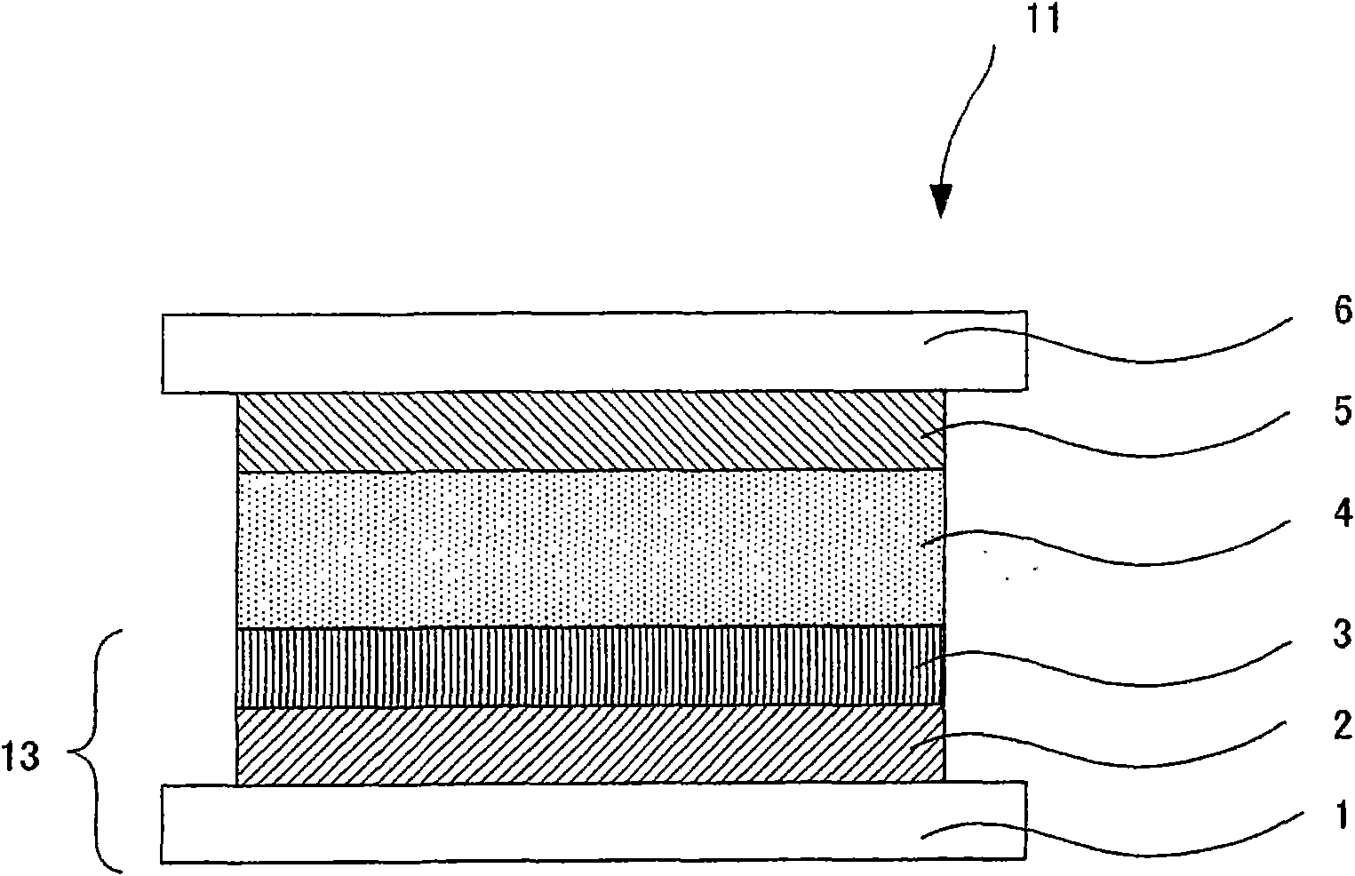
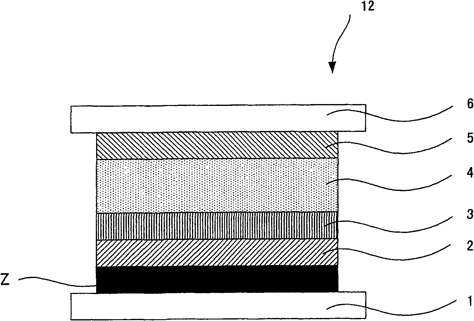
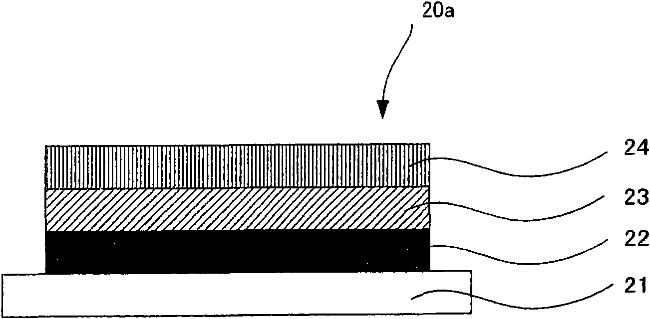
An oxide semiconductor electrode is provided with a base material; a bonding layer formed on the base material made of a thermoplastic resin; a first electrode layer formed on the bonding layer made of a metal oxide; and a porous layer formed on the first electrode and made of the fine particle of a metal oxide semiconductor, wherein the thermoplastic resin includes a silane-modified resin. The present invention further provides a method of producing an oxide semiconductor electrode. The method is characterized by comprising a step of forming a laminate for oxide semiconductor electrode, a step of forming an oxide semiconductor electrode having a heat-resistive substrate by carrying out the substrate forming step on the first electrode layer on the laminate for oxide semiconductor electrode, a step of peeling off the heat-resistive substrate on the oxide semiconductor electrode having heat-resistive substrate, wherein the step comprises: a step of forming pattern for sandwich layer, astep of forming a layer for oxide semiconductor layer, a step of forming a sandwic.

Description

[0001] This application is a divisional application, the application number of its parent application: 200610068365.3, the filing date: 2006.3.30, the name of the invention: oxide semiconductor electrodes, dye-sensitized solar cells and their manufacturing methods technical field [0002] The present invention relates to an oxide semiconductor electrode, a dye-sensitized solar cell using the same, and a method for producing the same. Background technique [0003] In recent years, environmental problems such as global warming caused by an increase in carbon dioxide have become serious, and countermeasures have been studied all over the world. Among them, research and development on solar cells utilizing the energy of sunlight as clean energy with little burden on the environment is actively underway. As such solar cells, monocrystalline silicon solar cells, polycrystalline silicon solar cells, amorphous silicon solar cells, and compound semiconductor solar cells have been put...

Claims


Application Information

Patent Timeline
Patent Type & Authority Applications(China)
IPC IPC(8): H01G9/04H01G9/20H01M14/00H01L51/44H01L51/42H01L51/48
CPCY02E10/542Y02E10/52Y02E10/549Y02P70/50
Inventor 薮内庸介中川博喜小堀裕之
Owner DAI NIPPON PRINTING CO LTD
Learn More