Near-infrared reflective transparent conductive film and preparation method thereof
A transparent conductive film, near-infrared technology, applied in cable/conductor manufacturing, chemical instruments and methods, conductive layers on insulating carriers, etc., can solve the problems of metal films with low near-infrared reflection efficiency and weak visible light transmission performance, Achieve the effect of easy deposition system, simple method and operation of deposition system
- Summary
- Abstract
- Description
- Claims
- Application Information
AI Technical Summary
Problems solved by technology
Method used
Image
Examples
Embodiment 1
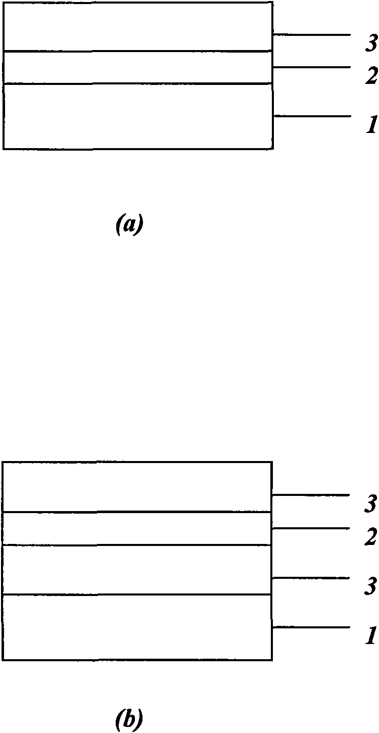
[0032] Embodiment 1: the preparation method of Cu / AZO near-infrared reflective transparent conductive film
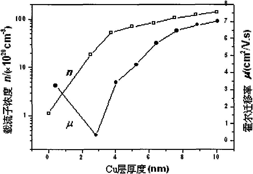
[0033] Clean the glass substrate and place it on the sample holder in the reaction chamber of the magnetron sputtering device, with the substrate deposition surface facing down, which can effectively prevent the contamination of the substrate surface by granular impurities, and the vacuum degree of the reaction chamber is pumped to 3× 10 -3 Pa, with Cu metal as the target material and pure Ar as the sputtering gas into the reaction chamber, the metal Cu layer was deposited by DC reactive magnetron sputtering. The gas pressure is 1.0Pa, the sputtering power is 120W, and the substrate temperature is normal temperature to carry out deposition and growth. The film thickness is determined by the growth time, monitored in real time by an oscillating film thickness monitor, and accurately measured by an ellipsometer.
[0034] After the sputtering of the metal Cu layer is com...
Embodiment 2
[0037] Embodiment 2: the preparation method of AZO / Cu / AZO multilayer transparent conductive film
[0038] Clean the glass substrate and place it on the sample holder in the reaction chamber of the magnetron sputtering device, with the substrate deposition surface facing down, which can effectively prevent the contamination of the substrate surface by granular impurities, and the vacuum degree of the reaction chamber is pumped to 3× 10 -3 Pa, with the (Zn+Al) alloy containing 4% Al as the target material, with pure Ar and pure O 2 As the sputtering gas was input into the reaction chamber, the transparent AZO layer was deposited by DC reactive magnetron sputtering. Ar:O 2 =12:1, the gas pressure is 1.0Pa, the sputtering power is 140W, and the substrate temperature is normal temperature, and deposition and growth are carried out. The thickness of the transparent AZO layer is 30nm.
[0039] After the first transparent ZnO layer is sputtered, Cu metal is used as the target mate...
Embodiment 3
[0043] Embodiment 3: Cu (7.5nm) / AZO (60nm) annealing
[0044] The near-infrared reflective transparent conductive film of the Cu (7.5nm) / AZO (60nm) structure obtained in Example 1 is annealed in a vacuum environment, and the annealing vacuum degree is 3 × 10 -3 Pa, the annealing time is 45 minutes, and the annealing temperature is 400°C.
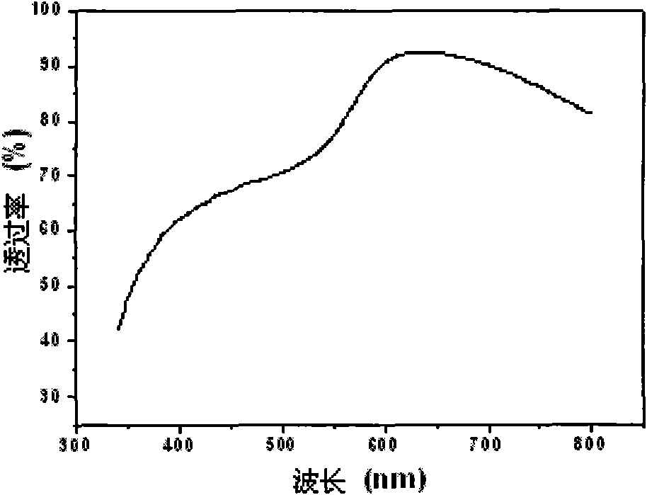
[0045] The visible light transmission spectrum and optical reflection spectrum of the near-infrared reflective transparent conductive film of Cu(7.5nm) / AZO(60nm) structure after annealing are as follows: image 3 and 4 shown. The photoelectric performance index of the thin film structure is as follows:
[0046] Resistivity
PUM
| Property | Measurement | Unit |
|---|---|---|
| thickness | aaaaa | aaaaa |
| thickness | aaaaa | aaaaa |
| electrical resistivity | aaaaa | aaaaa |
Abstract
Description
Claims
Application Information
 - R&D
- Intellectual Property
- Life Sciences
- Materials
- Tech Scout
- Unparalleled Data Quality
- Higher Quality Content
- 60% Fewer Hallucinations
Browse by: Latest US Patents, China's latest patents, Technical Efficacy Thesaurus, Application Domain, Technology Topic, Popular Technical Reports.
© 2025 PatSnap. All rights reserved.Legal|Privacy policy|Modern Slavery Act Transparency Statement|Sitemap|About US| Contact US: help@patsnap.com


