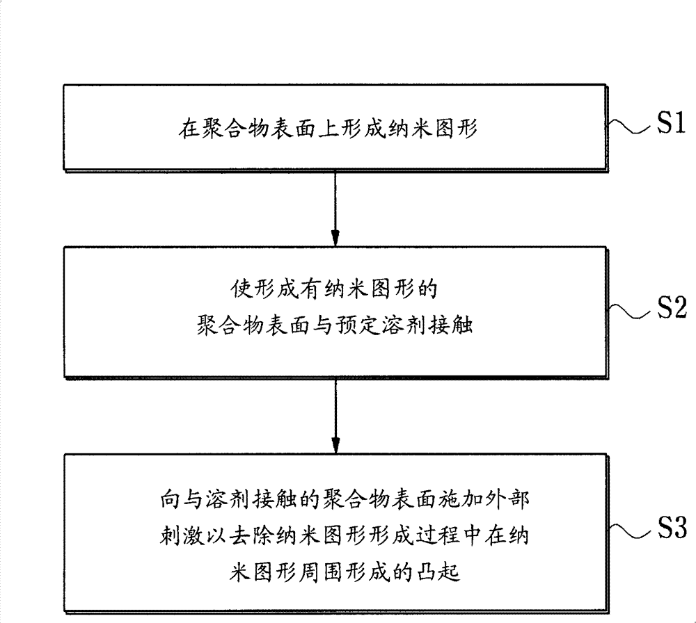
Removal of bulge effect in nano patterning
A nano-patterning and nano-indentation technology, applied in nanotechnology, nanotechnology, nanostructure manufacturing, etc., can solve the problems of complexity, limitation, and expensive methods.
- Summary
- Abstract
- Description
- Claims
- Application Information
AI Technical Summary
Problems solved by technology
Method used
Image

Examples
Embodiment 1
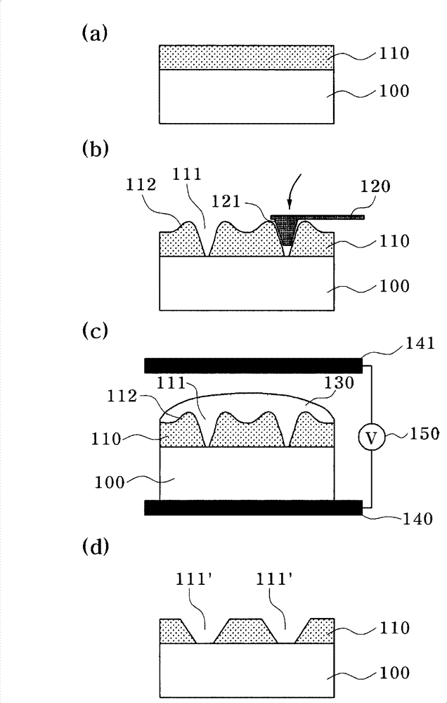
[0092] Fabrication of nanostructures with protrusions removed by applying an electric field
[0093] (a) Coating PMMA on the substrate
[0094] The silicon substrate was cleaned by sonication using acetone, and a 4 wt% solution of PMMA with a molecular weight of 950K (950K C4) dissolved in chlorobenzene solvent was spin-coated on the silicon substrate. Then it was soft-baked in an oven at 170° C. for 30 minutes to obtain a substrate coated with a PMMA film without pinholes. According to AFM measurement, the film thickness is 500 nm, and the RMS roughness is 0.6 nm.
[0095] (b) Dimple formation by nanoindentation
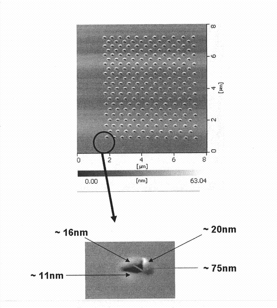
[0096] Surface modification, ie, nanoindentation, was performed on the PMMA film using a commercially available AFM device (SPA-400, Seiko Instruments, Japan). Nanoindentation was performed in tapping mode using a pyramidal silicon probe (PPP-NCHR, Nanosensors, Switzerland) with a tip diameter of 10 nm, a spring constant of 42 N / m, and a resonance frequency of ...
Embodiment 2
[0101] Fabrication of nanostructures with protrusions removed by applying ultrasound
[0102] Nanoindentation was performed under the same conditions as in (a) and (b) of Example 1 to form concave holes, except that the following silicon substrate was used, which was dissolved by using 2% by weight of A solution of PMMA with a molecular weight of 950K (950KA2) in anisole instead of chlorobenzene was coated with a film with a thickness of 70 nm and an RMS roughness of 0.6 nm.
[0103] Using an ultrasonic treatment device (JAC Ultrasonic 1002, frequency = 40 KHz, power = 125 W, KODO Technical Research), ultrasonic waves were applied in a solvent with a DI:IPA ratio of 1:5 for 5 minutes.
[0104] In addition, nanoindentation as described above was performed to form triangular, rectangular, and hexagonal nanopatterns composed of continuous lines, and ultrasonic waves were applied for 5 minutes in a solvent with a DI:IPA ratio of 1:5.
[0105] Observing the surface before and af...
PUM
| Property | Measurement | Unit |
|---|---|---|
| diameter | aaaaa | aaaaa |
| thickness | aaaaa | aaaaa |
| surface roughness | aaaaa | aaaaa |
Abstract
Description
Claims
Application Information
 - R&D
- Intellectual Property
- Life Sciences
- Materials
- Tech Scout
- Unparalleled Data Quality
- Higher Quality Content
- 60% Fewer Hallucinations
Browse by: Latest US Patents, China's latest patents, Technical Efficacy Thesaurus, Application Domain, Technology Topic, Popular Technical Reports.
© 2025 PatSnap. All rights reserved.Legal|Privacy policy|Modern Slavery Act Transparency Statement|Sitemap|About US| Contact US: help@patsnap.com