Method for manufacturing a semiconductor device, method and structure for mounting the semiconductor device

An installation method and installation structure technology, which are applied in the fields of semiconductor/solid-state device manufacturing, semiconductor devices, and semiconductor/solid-state device components, etc., can solve the problems of reduced productivity of semiconductor devices, reduced connection reliability, low elastic modulus, etc. The effect of connection reliability, suppression of disconnection, and productivity improvement

Inactive Publication Date: 2009-10-21
SEIKO EPSON CORP
View PDF4 Cites 1 Cited by
  • Summary
  • Abstract
  • Description
  • Claims
  • Application Information

AI Technical Summary

Problems solved by technology

However, if the shape of the protrusion is controlled by curing the photosensitive insulating resin by exposure to ultraviolet rays, the exposure conditions will change due to the deterioration of the exposure lamp, making it difficult to control the shape.
As a result, there is a problem that the productivity of the semiconductor device is lowered.
[0008] Furthermore, it is considered that if a resin with a low elastic modulus such as silicon is used for the resin forming the core of the protruding electrode, the resin forming the core of the protruding electrode will be larger than necessary due to the conditions of the pressurization process during mounting. Deformation, resulting in disconnection of the wiring of the protruding electrode
Also in this case, there is a problem that the connection reliability between the protruding electrodes of the driving IC and the terminal electrodes on the substrate is reduced.

Method used


Image

  • Method for manufacturing a semiconductor device, method and structure for mounting the semiconductor device
  • Method for manufacturing a semiconductor device, method and structure for mounting the semiconductor device
  • Method for manufacturing a semiconductor device, method and structure for mounting the semiconductor device

Examples


Embodiment Construction

[0041] One embodiment of the invention will be described below with reference to the drawings.

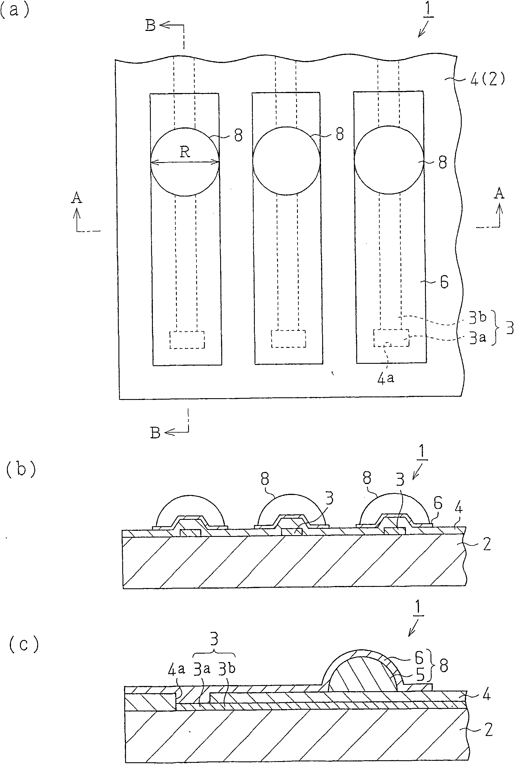
[0042] First, the semiconductor device 1 of the present invention will be described. figure 1 (a) is a plan view of main parts of the semiconductor device 1 of the liquid crystal display device. and, figure 1 (b) is figure 1 A-A line sectional view in (a), figure 1 (c) is figure 1 B-B line sectional view in (a).

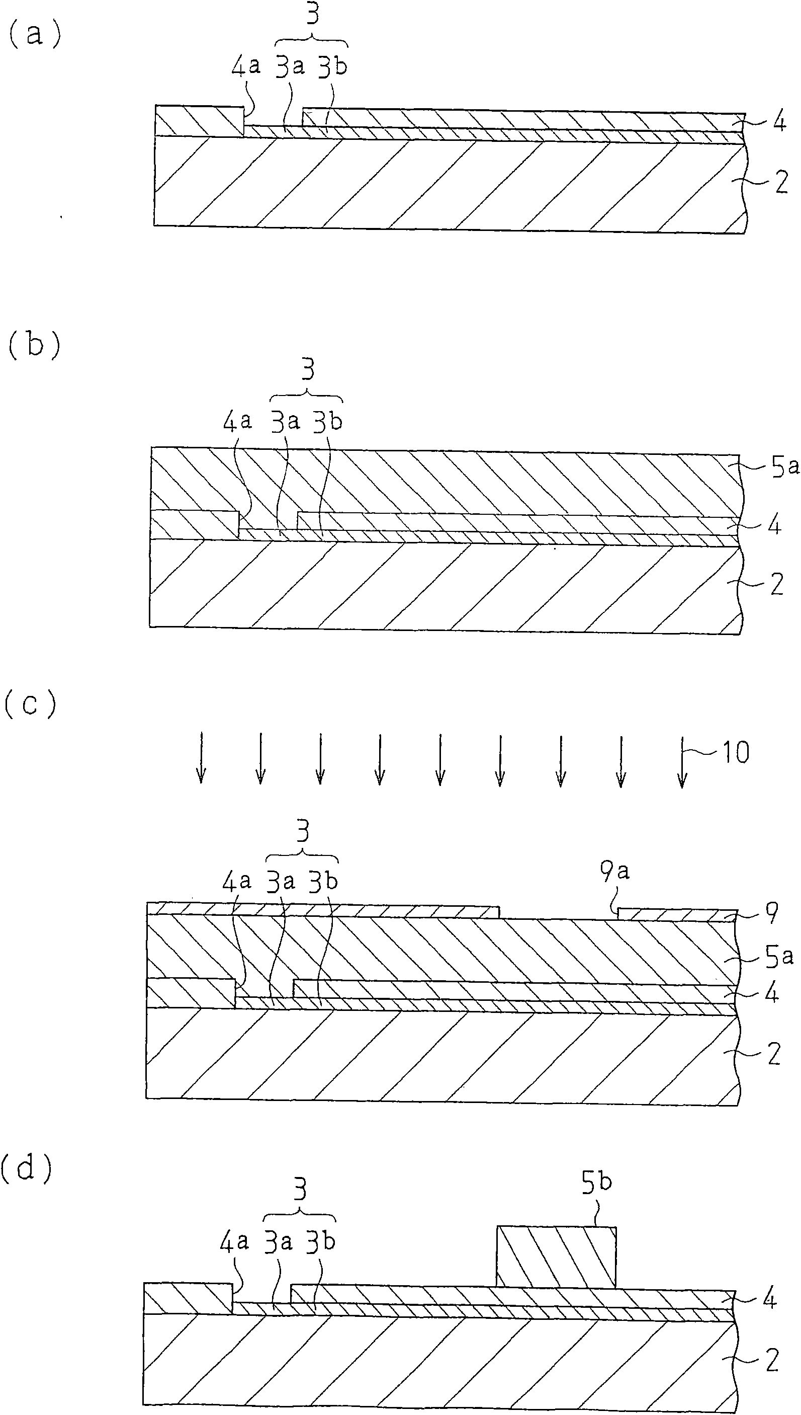
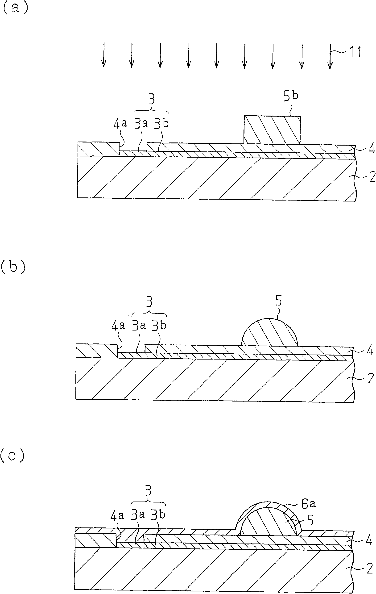
[0043] Such as figure 1 (a)~ figure 1 As shown in (c), in the semiconductor device 1 , a plurality of electrodes 3 are formed on the semiconductor substrate 2 . Each electrode 3 is an electrode for inputting and outputting electric signals, and includes an electrode pad 3 a and a wiring 3 b connected to the electrode pad 3 a. In this embodiment, a plurality of electrodes 3 are formed near the edge of the semiconductor substrate 2 at a predetermined pitch, and the material of each electrode 3 is aluminum.

[0044] Also, these electrodes 3 are covered with a protec...


PUM


Abstract

The present invention provides a method for manufacturing a semiconductor device for improving a productivity of the semiconductor device, a method and a structure for mounting the semiconductor device. A protective layer (4) is coated with an acroid resin which is used as a light-sensitive resin for forming a bulging body (5), to form a resin layer. On the resin layer, a mask having an opening portion is located at a prescribed position, further part of the resin layer exposing from the opening portion is exposed by irradiating ultraviolet on the mask. By means of solidifying the resin through the ultraviolet, a cylinder-shaped bulging body (5b) having a plane top is formed. Then, the ultraviolet (11) is irradiated on the bulging body (5b) to heat the bulging body (5b), such that the acroid resin for forming the bulging body (5b) is melted. Due to a surface tension generated on the melted resin, the top of the planar bulging body (5b) is deformed into a smooth curved face. thereby a near-hemisphere-shaped bulging body (5) is formed from the bulging body (5b).

Description

[0001] The present invention is a divisional application of the application number 200610068103.7 filed by the applicant Seiko Epson Co., Ltd. on March 21, 2006, and the title of the invention is "Semiconductor device manufacturing method, semiconductor device installation method and installation structure". technical field [0002] The present invention relates to a manufacturing method of a semiconductor device, a mounting method and a mounting structure of the semiconductor device. Background technique [0003] Conventionally, COG (Chip On Glass) connection is known as a connection method for mounting a driving IC on a display device substrate. In this COG connection, for example, Au-plated bumps (hereinafter simply referred to as bumps) as electrodes are formed on the driving IC. Then, a mounting method is employed in which the bumps formed on the driver IC and the bumps formed on the The terminal electrodes on the substrate of the display device are electrically connec...

Claims


Application Information

Patent Timeline
Patent Type & Authority Applications(China)
IPC IPC(8): H01L21/60H01L23/488
CPCH01L2924/14H01L2224/83192H01L2224/16225H01L2224/73204H01L2224/32225
Inventor 田中秀一
Owner SEIKO EPSON CORP
Why Eureka
Try Eureka