Method of planarizing solid surface with gas cluster ion beam and solid surface planarizing apparatus
一种平坦化方法、气体团簇的技术,应用在半导体/固态器件制造、电气元件、放电管等方向,能够解决不容易等问题
- Summary
- Abstract
- Description
- Claims
- Application Information
AI Technical Summary
Problems solved by technology
Method used
Image

Examples
no. 1 example
[0099] according to Figure 7 The flow chart shows the process of planarizing the target plane in the planarized pattern structure. From a different point of view, the planarization of the target surface is the etching of the target surface. In this example, trimming of the pattern structure and planarization of the target surface is carried out by etching the target surface.
[0100] This process will now be described.
[0101] Step S1
[0102] Before the GCIB irradiation, the pattern structure (fine structure) of the target 19 is observed by an atomic force microscope or the like, and shape data is obtained.
[0103] Step S2
[0104] Based on the difference between the shape data and desired values such as pattern width, etc., the amount of etching required to form a fine structure of a desired size is calculated.
[0105] Step S3
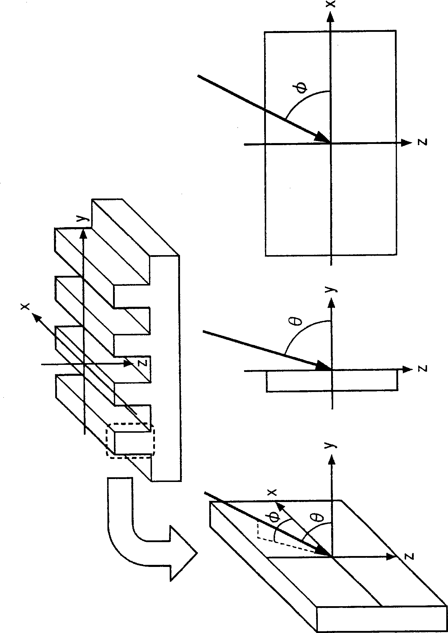
[0106] The target 19 is attached to the target support 18 of the solid surface planarization apparatus 100, and the angles of the target...
no. 2 example
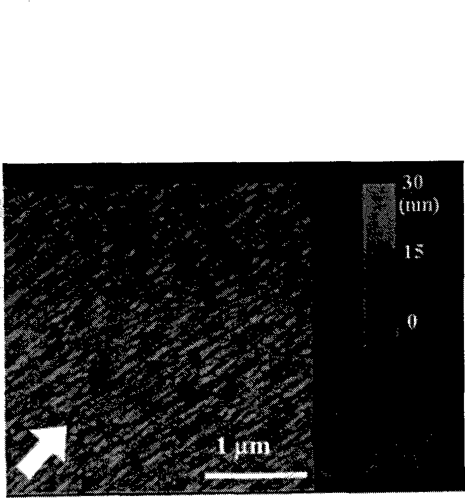
[0120] The same experiment as in the first example was performed except that the irradiation inclination angle φ was 0°. Irradiation at 0° irradiation inclination φ corresponds to GCIB irradiation in a direction parallel to the stripe formed by Ar ion milling on the side of the wire (see image 3 angle definition in ). Figure 13A AFM image of the side of the wire after GCIB irradiation at an irradiation angle θ of 83° is shown. Figure 13A Arrows in indicate SF 6 Projected irradiation direction of (sulfur hexafluoride) GCIB irradiation. The figure shows SF 6 The uneven shape found before GCIB irradiation was not eliminated. Right along the white line ( Figure 13A ) for detailed observation of the uneven shapes in the cross-section, it was found that after GCIB irradiation, the short-interval uneven shapes located on the long-interval uneven shapes disappeared and left smooth curves (such as Figure 13B shown in the oval box). Further analysis of the FFT spectral lines...
no. 3 example
[0122] An experiment was conducted to check whether the effect observed in the first embodiment could be seen by combining another material with gas clusters, an Ar gas cluster ion beam directed to an observation sample of a Cr film formed on a silicon substrate.
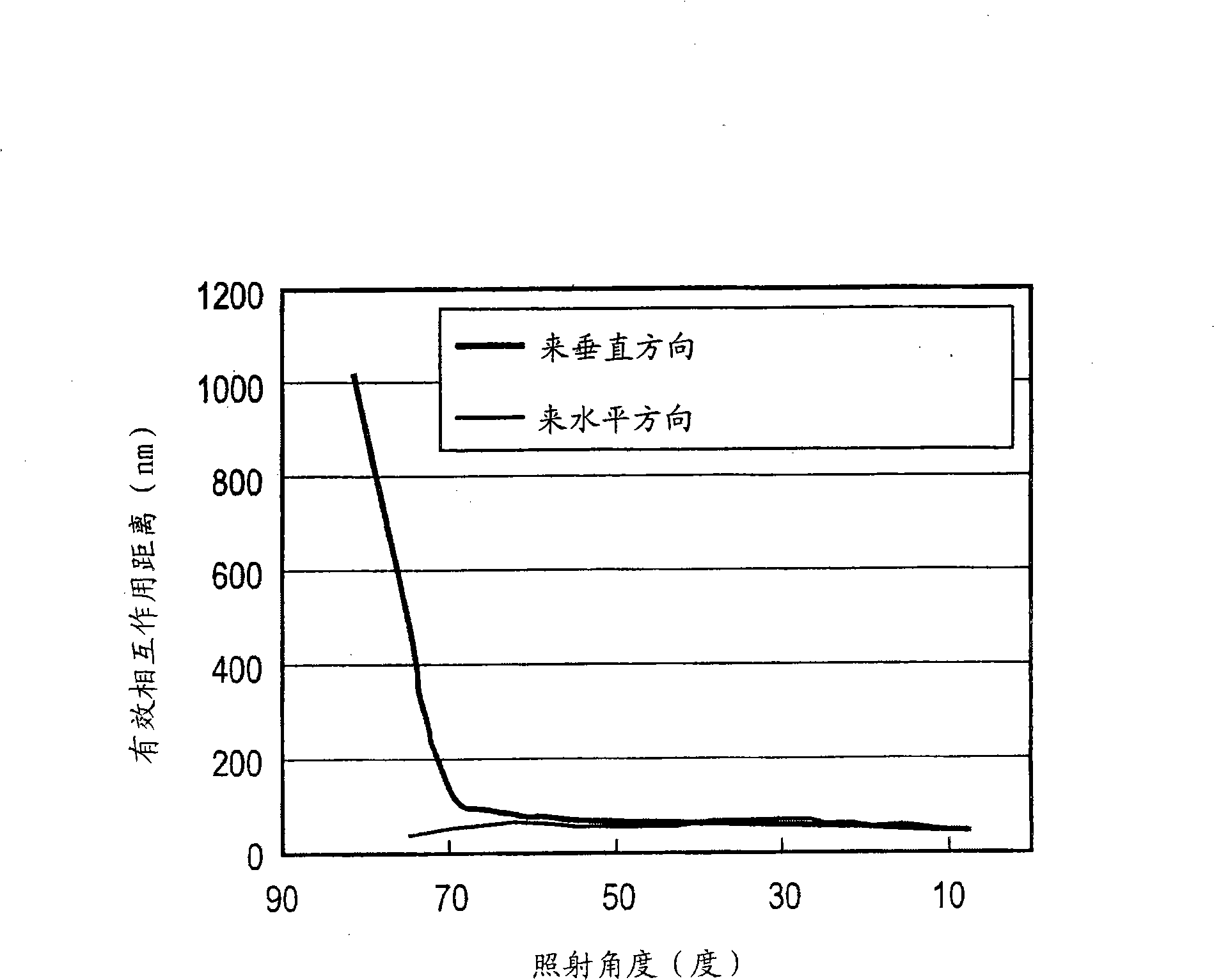
[0123] The same Ar ion milling conditions as those employed in etching the line-space pattern structure on the surface of the silicon substrate in the first example were employed and the same striped structure was observed in the Cr film observation sample. For the Cr film observation sample, the relationship between the irradiation angle θ of the Ar gas cluster ion beam and the average surface roughness Ra was detected. According to the relationship between the irradiation angle θ and the dose required for 50nm etching of the Cr film stored in the database ( Figure 14 ) to determine the irradiation dose (acceleration energy is 30 keV, cluster particle size distribution has a peak of 2000 particles per cluster). ...
PUM
 Abstract
Description
Claims
Application Information
 - R&D
- Intellectual Property
- Life Sciences
- Materials
- Tech Scout
- Unparalleled Data Quality
- Higher Quality Content
- 60% Fewer Hallucinations
Browse by: Latest US Patents, China's latest patents, Technical Efficacy Thesaurus, Application Domain, Technology Topic, Popular Technical Reports.
© 2025 PatSnap. All rights reserved.Legal|Privacy policy|Modern Slavery Act Transparency Statement|Sitemap|About US| Contact US: help@patsnap.com