
A device with a packaging structure of a Love wave sensor

A packaging structure and sensor technology, applied in the direction of electrical components, impedance networks, etc., can solve the problems of increased insertion loss, decreased sensor repeatability, accuracy and reliability, difficulty in protecting interdigital transducers, etc., to achieve improved repeatability Sexuality, consumption saving and loss reduction effect

Inactive Publication Date: 2011-12-07
INST OF ACOUSTICS CHINESE ACAD OF SCI
View PDF0 Cites 0 Cited by
  • Summary
  • Abstract
  • Description
  • Claims
  • Application Information

AI Technical Summary

Problems solved by technology

The conventional Love wave sensor structure is difficult to protect the performance of the interdigital transducer from the influence of the analyte, resulting in increased insertion loss, and this structure is not conducive to controlling the sample injection, reaction, and separation of the analyte, resulting in the loss of the entire sensor Repeatability, accuracy and reliability decrease

Method used


Image

  • A device with a packaging structure of a Love wave sensor
  • A device with a packaging structure of a Love wave sensor
  • A device with a packaging structure of a Love wave sensor

Examples


Embodiment Construction

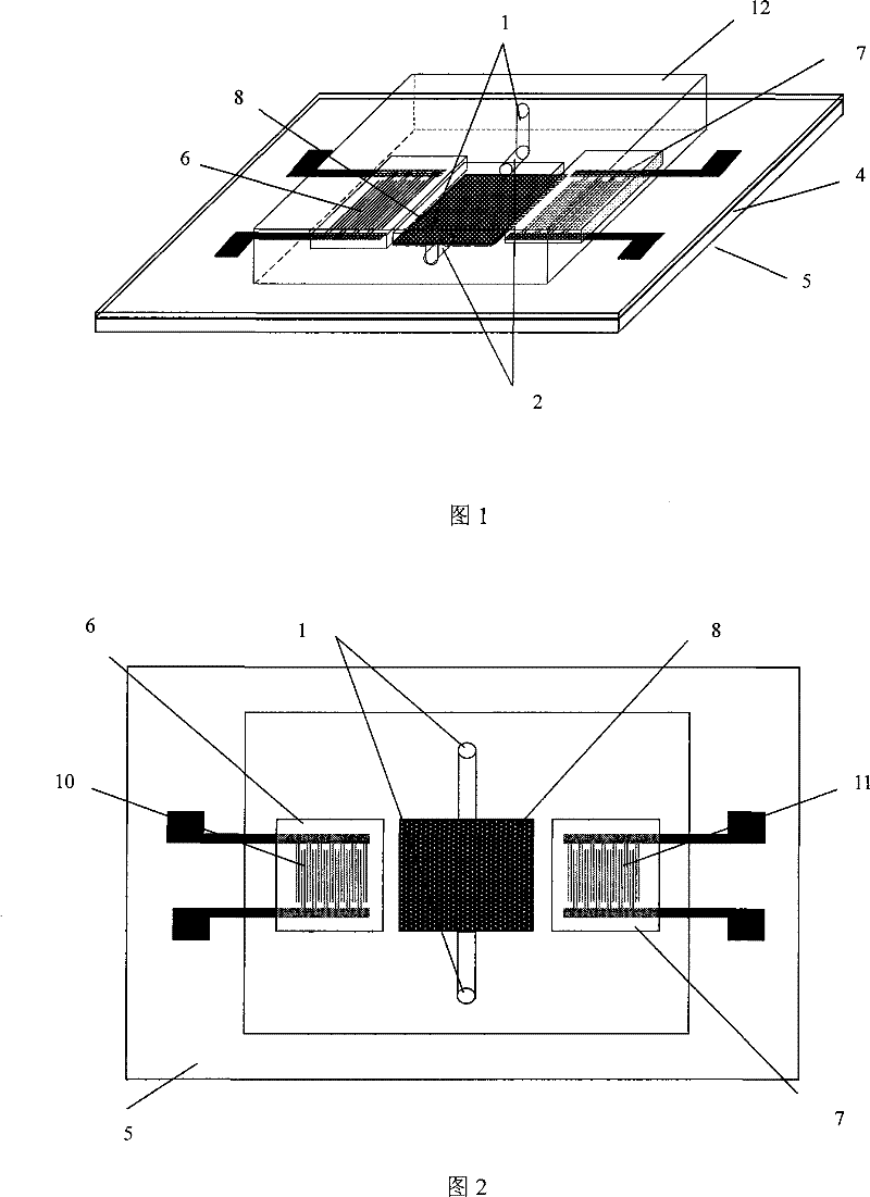
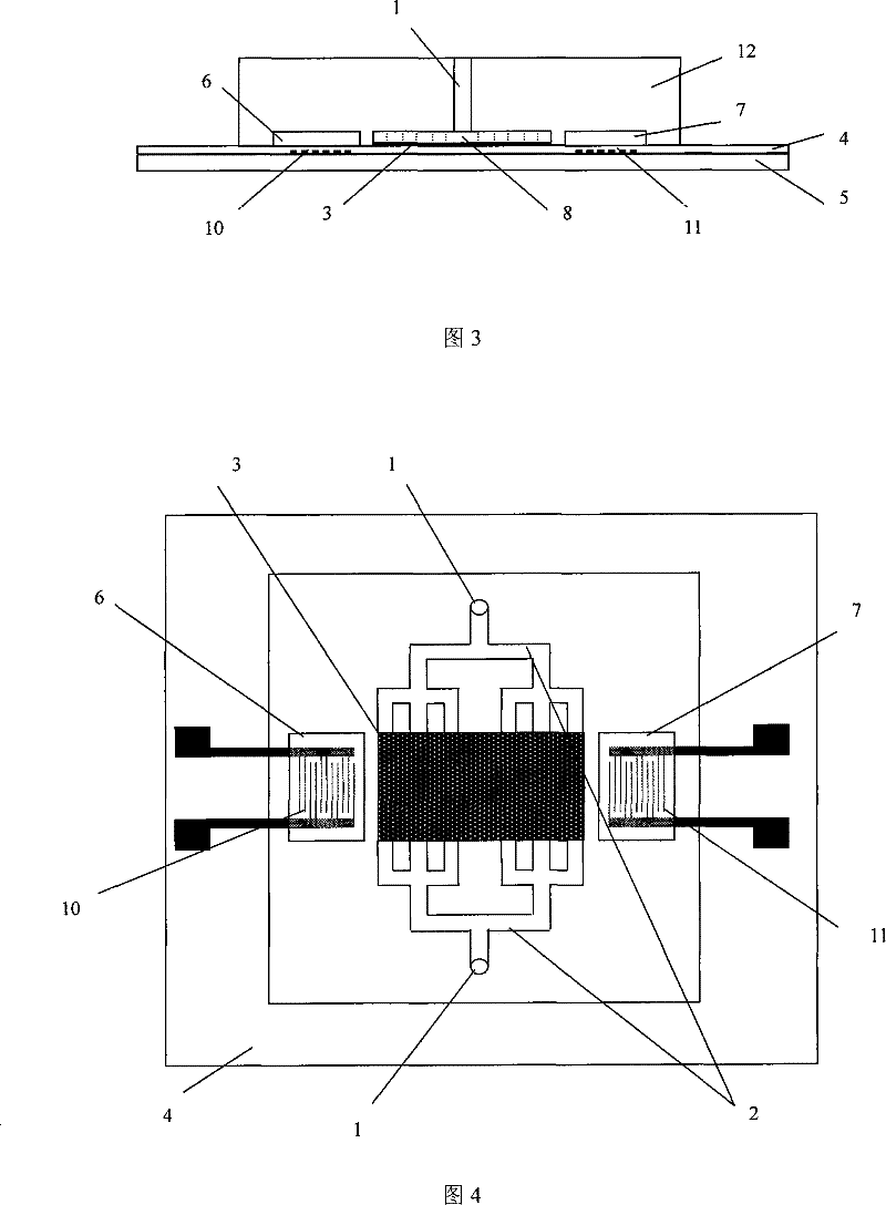
[0028] Specifically make the structure according to the technical scheme of the present invention, see Figure 1~3 , consists of Love wave sensor and microfluidic chip.

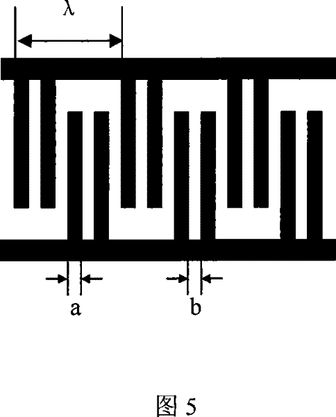
[0029] Love wave sensor structures such as image 3 As shown, it includes: a piezoelectric substrate 5 , a covering waveguide layer 4 , a sensitive film 3 , an input IDT 10 and an output IDT 11 . In this embodiment, the piezoelectric substrate of the Love wave sensor is made of St-cut 90-degree quartz material with a thickness of 0.5mm; the input and output interdigital transducers 10, 11 all adopt a split-finger structure, such as Figure 5 As shown, the period λ is 40 microns, the number of periods is 60, the material of the fingers is aluminum, the thickness of the fingers is 1500 angstroms, the width a of the fingers and the spacing b of the fingers are both one-eighth wavelength; the aperture is 2 mm; Transducer center frequency f 0 =124 MHz; the waveguide layer 4 is made of silicon dioxide, with a th...


PUM


Abstract

The invention relates to a device with a package structure of a Love wave sensor, comprising a Love wave sensor, wherein the input interdigital transducer and the output interdigital transducer of the Love wave sensor are located on the left and right sides of a sensitive membrane , which is characterized in that: it also includes a microfluidic chip, which is correspondingly bonded to the Love wave sensor; a groove is provided on the contact surface of the microfluidic chip and the Love wave sensor, so as to harmonize with the music After the Fun Wave sensor is bonded, the input interdigital transducer cavity, the output interdigital transducer cavity and the sensitive membrane cavity are not connected to each other; the surface of the contact part of the microfluidic chip and the Love wave sensor is formed The upper and lower sides of the sensitive membrane are also provided with a number of microchannels, one end of the microchannel is connected to the cavity of the sensitive membrane, and the other end is connected to the through holes set on the microfluidic chip for the entry and exit of the object to be tested . The invention can effectively improve the repeatability, accuracy and reliability of the sensor.

Description

technical field [0001] The invention relates to the field of a Love-type acoustic wave sensor (abbreviated as Love-wave) sensor, in particular to a device with a packaging structure of a Love-type acoustic wave sensor. Background technique [0002] Love wave is a kind of acoustic wave, which is a surface shear shear wave propagating in a thin-layer acoustic waveguide on the surface of a piezoelectric substrate. The particle vibration direction of the Love wave is parallel to the basic surface, so when the substrate surface is in contact with the liquid load, the coupling with the load is very small. And because the thin-layer acoustic waveguide binds the Love wave energy on the surface, the Love wave is very sensitive to surface disturbance. In addition, the manufacturing process of the device is not complicated, the advantages of light weight and cheap price have attracted widespread attention. [0003] Existing Love wave sensor packaging structure, as described in three ...

Claims


Application Information

Patent Timeline
Patent Type & Authority Patents(China)
IPC IPC(8): H03H9/25H03H9/02
Inventor 李红浪陈烨何世堂
Owner INST OF ACOUSTICS CHINESE ACAD OF SCI
Learn More