Manufacture method for layer-adding circuit board

A manufacturing method and circuit board technology, applied in circuits, semiconductor/solid-state device manufacturing, electrical components, etc., can solve problems such as low wiring density, complex process, and inability to meet users, so as to reduce manufacturing costs and reduce the thickness of finished boards. Effect

Inactive Publication Date: 2012-03-07
BRIDGE SEMICON
View PDF5 Cites 0 Cited by
  • Summary
  • Abstract
  • Description
  • Claims
  • Application Information

AI Technical Summary

Problems solved by technology

However, this manufacturing method is not only difficult to manufacture the copper core substrate, but also has the same disadvantages as the above method, such as low wiring density and complicated process.
Therefore, it generally cannot meet the needs of users in actual use.

Method used


Image

  • Manufacture method for layer-adding circuit board
  • Manufacture method for layer-adding circuit board
  • Manufacture method for layer-adding circuit board

Examples


Embodiment Construction

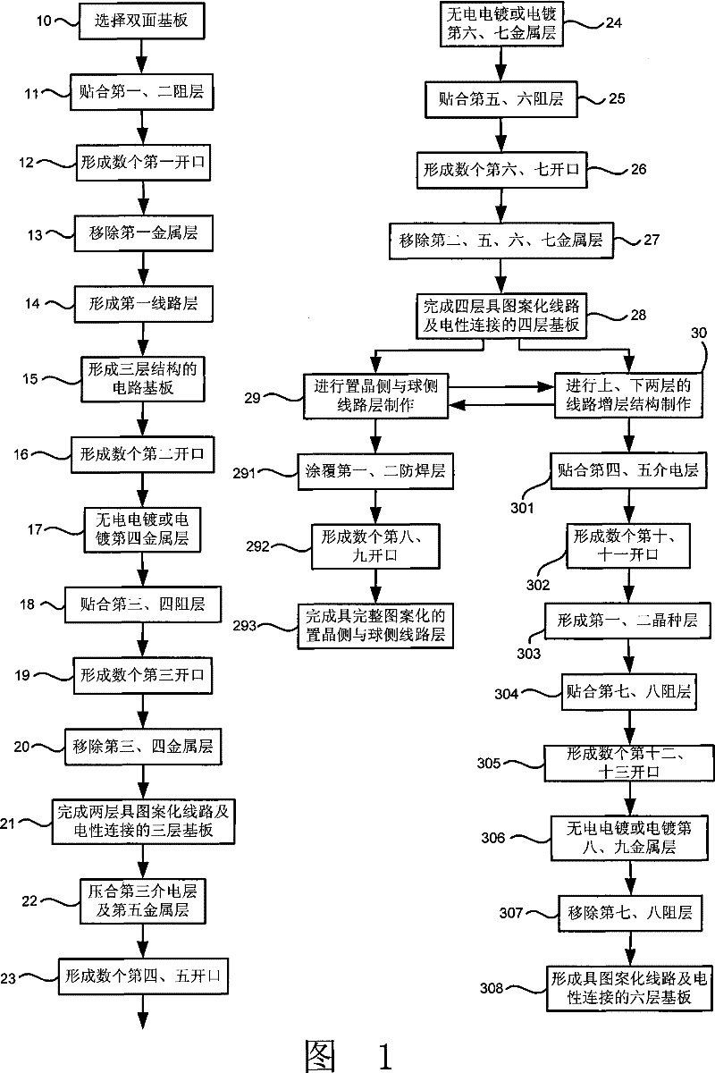
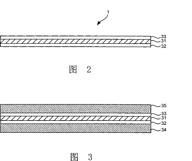
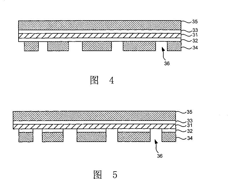
[0114] see Figure 1 to Figure 31 Shown are the schematic diagram of the production process of the present invention, the schematic cross-section of the double-sided substrate of the present invention, and the schematic cross-section of the two-layer substrate of the present invention. Figure 1 , The schematic cross-section of the two-layer substrate of the present invention Figure II , The schematic cross-section of the two-layer substrate of the present invention Figure three , The schematic cross-section of the two-layer substrate of the present invention Figure four , The schematic cross-section of the three-layer substrate of the present invention Figure 1 , The schematic cross-section of the three-layer substrate of the present invention Figure II , The schematic cross-section of the three-layer substrate of the present invention Figure three , The schematic cross-section of the three-layer substrate of the present invention Figure four , The schematic cross...


PUM


Abstract

The invention discloses a manufacture method for a layer-adding circuit board, which comprises the following steps that: a single layer circuit is manufactured by optical lithography and etching method and is taken as an electrically connected pad of a layer-adding structure, and a circuit board with a three-layer structure is formed on the connected pad surface in a pressing mode; a second layer-adding circuit is formed on the first layer-adding circuit structure, and a metal layer with the prior non-patterned circuit is formed into a third layer-adding circuit so as to form a four-layer substrate with a patterned circuit and electric connection; and the upper layer and the lower layer of the four-layer substrate are further taken as the electrically connected pads of the layer-adding structure respectively, or taken as a complete circuit between the wafer placing side and the ball side. Therefore, the method can effectively improve the problem of bow and twist of an ultrathin seed-layer substrate, simplify the manufacture flows of the conventional layer-adding circuit boards, and effectively reduce the thickness and the manufacturing cost of production boards.

Description

Technical field: [0001] The invention relates to a method for manufacturing a build-up circuit board, in particular to a method for manufacturing a build-up circuit board with a semiconductor multilayer packaging substrate structure based on a single-layer patterned circuit structure supported by a double dielectric layer. Background technique: [0002] In the production of general multi-layer packaging substrates, the production method usually starts with a core substrate, and then completes a double-sided structure of the inner core board through drilling, electroplating metal, plug holes, and double-sided circuit production. A multi-layer packaging substrate is then completed through a circuit build-up process. Such as Figure 32 As shown, it is a schematic cross-sectional view of a package substrate with a nucleated layer. First, a core substrate 81 is prepared, wherein the core substrate 81 is composed of a core layer 811 with a predetermined thickness and a circuit la...

Claims


Application Information

Patent Timeline
Patent Type & Authority Patents(China)
IPC IPC(8): H01L21/48
Inventor 林文强王家忠陈振重
Owner BRIDGE SEMICON
Why Eureka
Try Eureka