Copper core layer multilayer packaging substrate manufacturing method

A technique for encapsulating substrates and manufacturing methods, which is applied in the fields of multilayer circuit manufacturing, semiconductor/solid-state device manufacturing, electrical components, etc., and can solve problems such as difficulty in making copper core substrates, inability to meet user needs, and low wiring density, and achieve Improve the warping problem, simplify the packaging process, and improve the reliability

Inactive Publication Date: 2012-05-09
BRIDGE SEMICON
View PDF0 Cites 0 Cited by
  • Summary
  • Abstract
  • Description
  • Claims
  • Application Information

AI Technical Summary

Problems solved by technology

However, this manufacturing method is not only difficult to manufacture the copper core substrate, but also has the same disadvantages as the above method, such as low wiring density and complicated process.
Therefore, the general users cannot meet the needs of users in actual use

Method used


Image

  • Copper core layer multilayer packaging substrate manufacturing method
  • Copper core layer multilayer packaging substrate manufacturing method
  • Copper core layer multilayer packaging substrate manufacturing method

Examples


Embodiment Construction

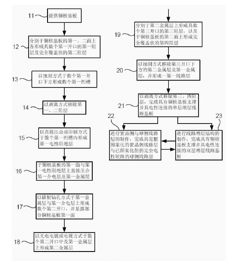
[0077] See figure 1 Shown is a schematic diagram of the production process of the present invention. As shown in the figure: the present invention is a manufacturing method of a copper core layer multilayer packaging substrate, which at least includes the following steps:

[0078] (A) Provide copper core substrate 11: Provide a copper core substrate;

[0079] (B) Forming the first and second resist layers and the first opening 12: respectively form a first resist layer on the first surface of the copper core substrate, and form a completely covered shape on the second surface of the copper core substrate And forming a plurality of first openings on the first resist layer by exposure and development methods;

[0080] (C) forming the first groove 13: forming a plurality of first grooves under the plurality of first openings by etching;

[0081] (D) Remove the first and second resist layers 14: remove the first resist layer and the second resist layer by peeling;

[0082] (E) Forming th...


PUM


Abstract

A copper core layer multilayer packaging substrate manufacturing method is a single surface and multilayer packaging substrate for starting manufacturing by taking the copper core substrate as a base. The structure comprises a thick copper plate with high rigidity, and one surface of the thick copper plate has a build-up circuit, while the other surface has a ball side pattern barrier. The mode for connecting its crystal providing side and ball side with various build-up circuits is that they are communicated by a plurality of electroplating blind holes and buried holes. Therefore, The inventive packaging substrate is characterized by including a high-density build-up circuits for providing the coiling required by connecting of electronic assembly, and simultaneously using a thick copper plate to provide enough rigidity to make the packaging process to be more easier. Therefore, the multilayer packaging substrate manufactured by the invention can form copper core layer multilayer packaging substrate supported by a copper core substrate, and can effectively improve plate bending problem of ultrathin nuclear layer substrate and simplify the making flow of conventional build-up circuit board, thereby achieving the object of improving the reliability when the packaging body is jointed to the substrate.

Description

Technical field: [0001] The invention relates to a manufacturing method of a copper core layer multilayer packaging substrate, in particular to a manufacturing method of a single-sided, multi-layer packaging substrate manufactured on the basis of a copper core substrate. Background technique: [0002] In the production of general multi-layer packaging substrates, the production method usually starts with a core substrate, through drilling, electroplating metal, plugging and double-sided circuit production, etc., to complete an inner core board with a double-sided structure. Then, a multi-layer package substrate is completed through a circuit build-up process. Such as Figure 22 As shown, it is a schematic cross-sectional view of a packaging substrate with a core layer. First, prepare a core substrate 60, wherein the core substrate 60 is composed of a core layer 601 with a predetermined thickness and a circuit layer 602 formed on the surface of the core layer 601, and a plurality ...

Claims


Application Information

Patent Timeline
Patent Type & Authority Patents(China)
IPC IPC(8): H05K3/46H01L21/48
Inventor 林文强王家忠陈振重
Owner BRIDGE SEMICON
Why Eureka
Try Eureka