Semiconductor device and semiconductor device manufacturing method
A manufacturing method and semiconductor technology, applied in semiconductor/solid-state device manufacturing, semiconductor devices, transistors, etc., can solve problems such as the gap between the insulating layer around the surface roughness of the gate electrode
- Summary
- Abstract
- Description
- Claims
- Application Information
AI Technical Summary
Problems solved by technology
Method used
Image
Examples
no. 1 example
[0120] [first embodiment]
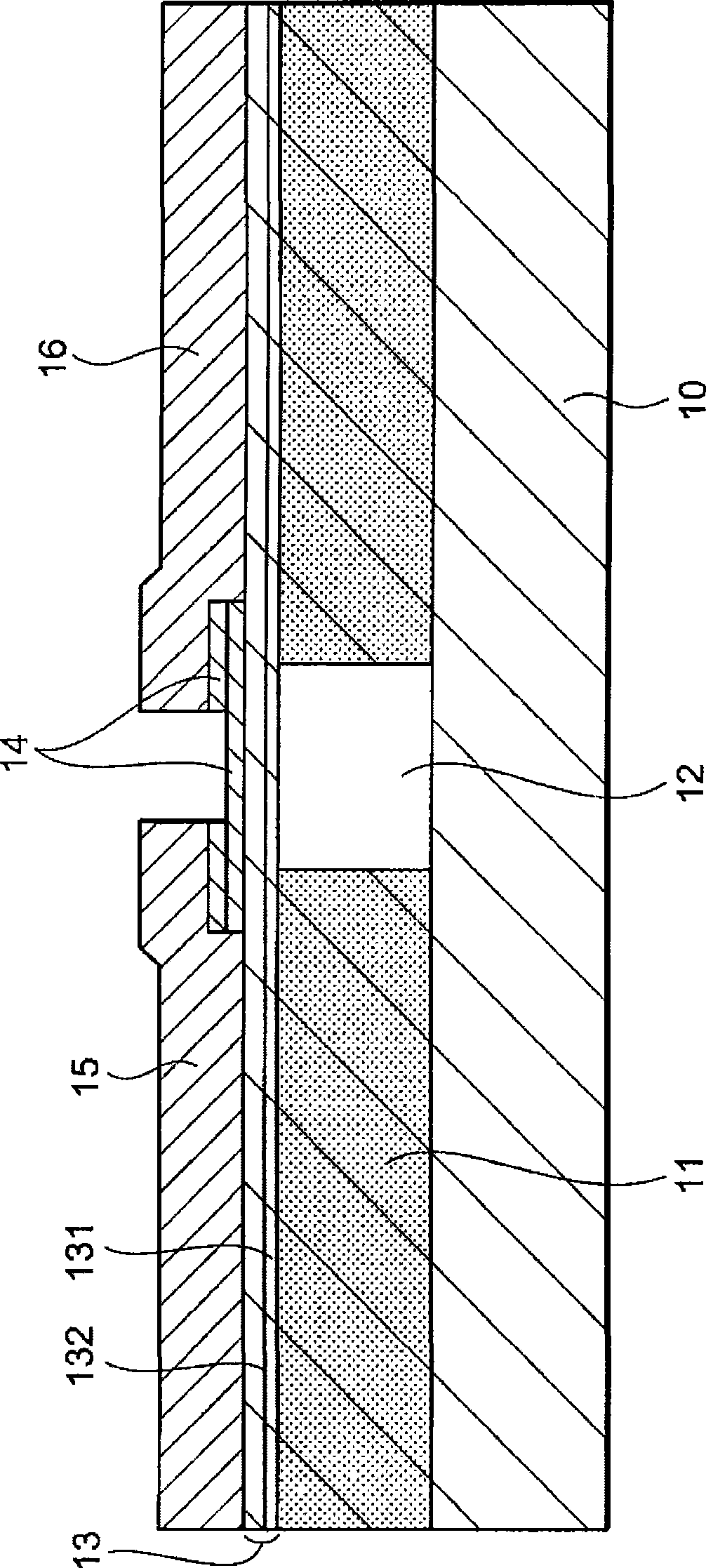
[0121] figure 1 A liquid crystal display device is applied and is a cross-sectional view showing an example of the structure of a thin film transistor (TFT: Thin Film Transistor) of the present invention. refer to figure 1 The thin film transistor has: a transparent resin film (insulator layer) 11 formed of a transparent photosensitive resin formed on a glass substrate (insulating substrate) 10; The gate electrode (conductor layer) 12 is substantially at the same height. The thin film transistor also has: a gate insulating film composed of an insulator coating film (overcoat film) 131 and a CVD dielectric film (insulator CVD film) 132 thereon formed on the entire transparent resin film 11 and the gate electrode 12. film 13 , semiconductor layer 14 formed on gate electrode 12 via gate insulating film 13 , source electrode 15 and drain electrode 16 connected to semiconductor layer 14 .
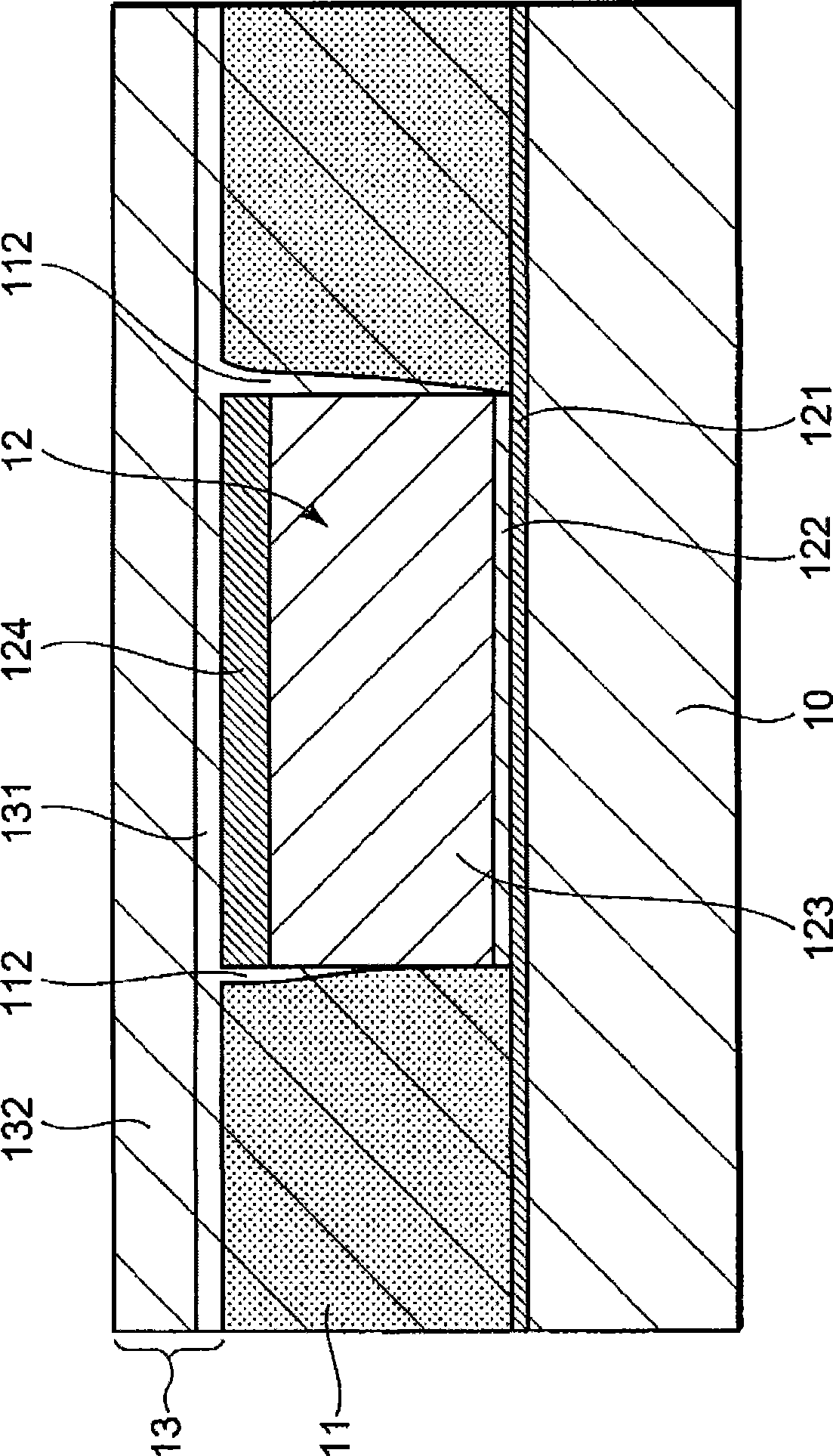
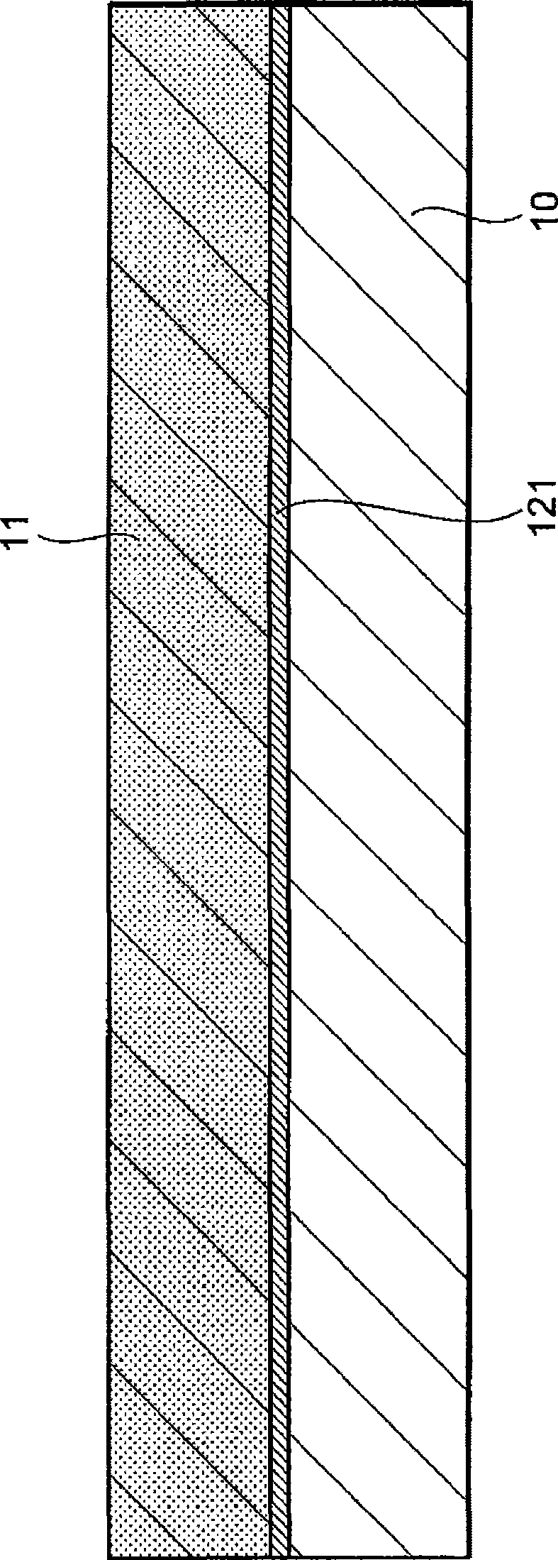
[0122] figure 2 It is an enlarged cross-sectional view sho...
no. 2 example
[0139] A second embodiment of the present invention will be described using the drawings.
[0140] Figure 9 Applicable to a liquid crystal display device, it is a cross-sectional view showing the structure of a thin film transistor (TFT) according to a second embodiment of the present invention. The thin film transistor has: a transparent resin film 11 made of a transparent photosensitive resin formed on a glass substrate (insulating substrate) 10; The gate electrode 12, the gate insulating film 133 made of an insulator coating film formed on the entire transparent resin film 11 and the gate electrode 12, the semiconductor layer 14 formed on the gate electrode 12 via the gate insulating film 133 , a source electrode 15 and a drain electrode 16 connected to the semiconductor layer 14 .
[0141] Figure 10 It is an enlarged cross-sectional view showing the structure of the gate electrode portion of the thin film transistor of the second embodiment. The illustrated gate elec...
no. 3 example
[0152] use Figure 16 A method for forming a thin film transistor according to a third embodiment of a liquid crystal display device will be described.
[0153] In the manufacturing method of the thin film transistor described in the second embodiment, the diffusion suppressing film 124 (thickness 0.1 μm) of nickel is formed on the copper layer 123, and after the gate electrode 12 is formed, the transparent resin film 11 is reached from the surface of the gate electrode 12. The entire area of the surface is made of Si in a microwave-excited RLSA plasma treatment device 3 N 4 The film (silicon nitride dielectric film) 132 is grown by CVD to form an insulating film. Then at Si 3 N 4 The entire film is coated to form an insulator coating film 131 to form a gate insulating film 13 . The insulator coating film 131 is obtained by coating a liquid in which an Si organic compound, that is, an organosiloxane, is dissolved in an organic solvent (propylene glycol monomethyl ether)...
PUM
| Property | Measurement | Unit |
|---|---|---|
| Flatness | aaaaa | aaaaa |
| Flatness | aaaaa | aaaaa |
| Thickness | aaaaa | aaaaa |
Abstract
Description
Claims
Application Information
 - Generate Ideas
- Intellectual Property
- Life Sciences
- Materials
- Tech Scout
- Unparalleled Data Quality
- Higher Quality Content
- 60% Fewer Hallucinations
Browse by: Latest US Patents, China's latest patents, Technical Efficacy Thesaurus, Application Domain, Technology Topic, Popular Technical Reports.
© 2025 PatSnap. All rights reserved.Legal|Privacy policy|Modern Slavery Act Transparency Statement|Sitemap|About US| Contact US: help@patsnap.com


