
Manufacturing method for multilayered rigidity and flexibility combined printed circuit board

A technology of printed circuit board and manufacturing method, applied in the direction of multi-layer circuit manufacturing, etc., can solve the problems of increasing manufacturing cost, deviation of fit, and high processing cost, avoiding dislocation during processing, improving performance reliability, and qualifying products. rate increase effect

Active Publication Date: 2009-08-12
吉安新宇腾跃电子有限公司
View PDF0 Cites 38 Cited by
  • Summary
  • Abstract
  • Description
  • Claims
  • Application Information

AI Technical Summary

Problems solved by technology

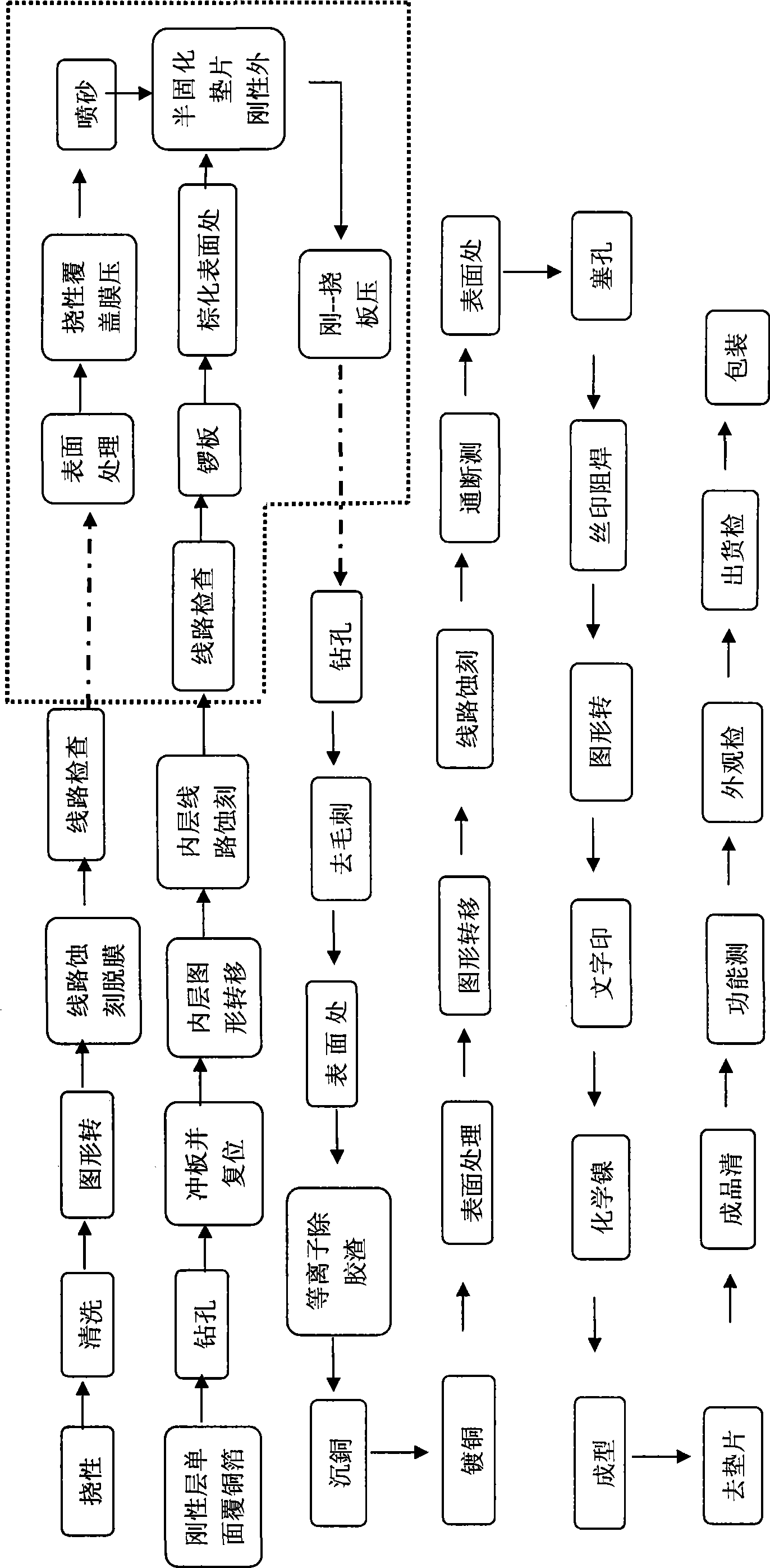
like figure 1 As shown, the rigid part adopts the gong plate (that is, processed by a CNC milling machine) to process the filling piece, and the filling piece of the epoxy resin plate is separately milled into a layered filling area. The disadvantages are: (1) It will cause The generated dust increases, pollutes the surface of the product, needs to increase the cleaning process, increases the cost, and the quality is also affected to a certain extent; (2) Because the diameter of the milling cutter has a certain width, the area of ​​the filling piece is reduced after processing, and the filling piece It cannot be used for filling the original area, so it is necessary to reuse the epoxy resin board of the same specification to process the same size filler piece to fill the empty slot of the rigid-flex printed circuit board, which not only wastes materials but also increases manufacturing costs, and the efficiency is greatly reduced. And there are also deviations in the degree of fit; (3) due to the need for manual single-piece filling, the efficiency is low, and it is uneven, the standard is not uniform, and it is easy to cause artificial quality effects; (4) because the filling gap is uneven or there are seams, the The surface of the product is polluted during liquid etching and micro-acid cleaning, and it is difficult to clean it with equipment because it seeps into the groove area of ​​the rigid-flex printed circuit board. In addition, oil seepage occurs during silk screen printing green oil solder mask, causing the filled area to be covered with ink Contamination, and solidification when cured at high temperature, and cannot be cleaned
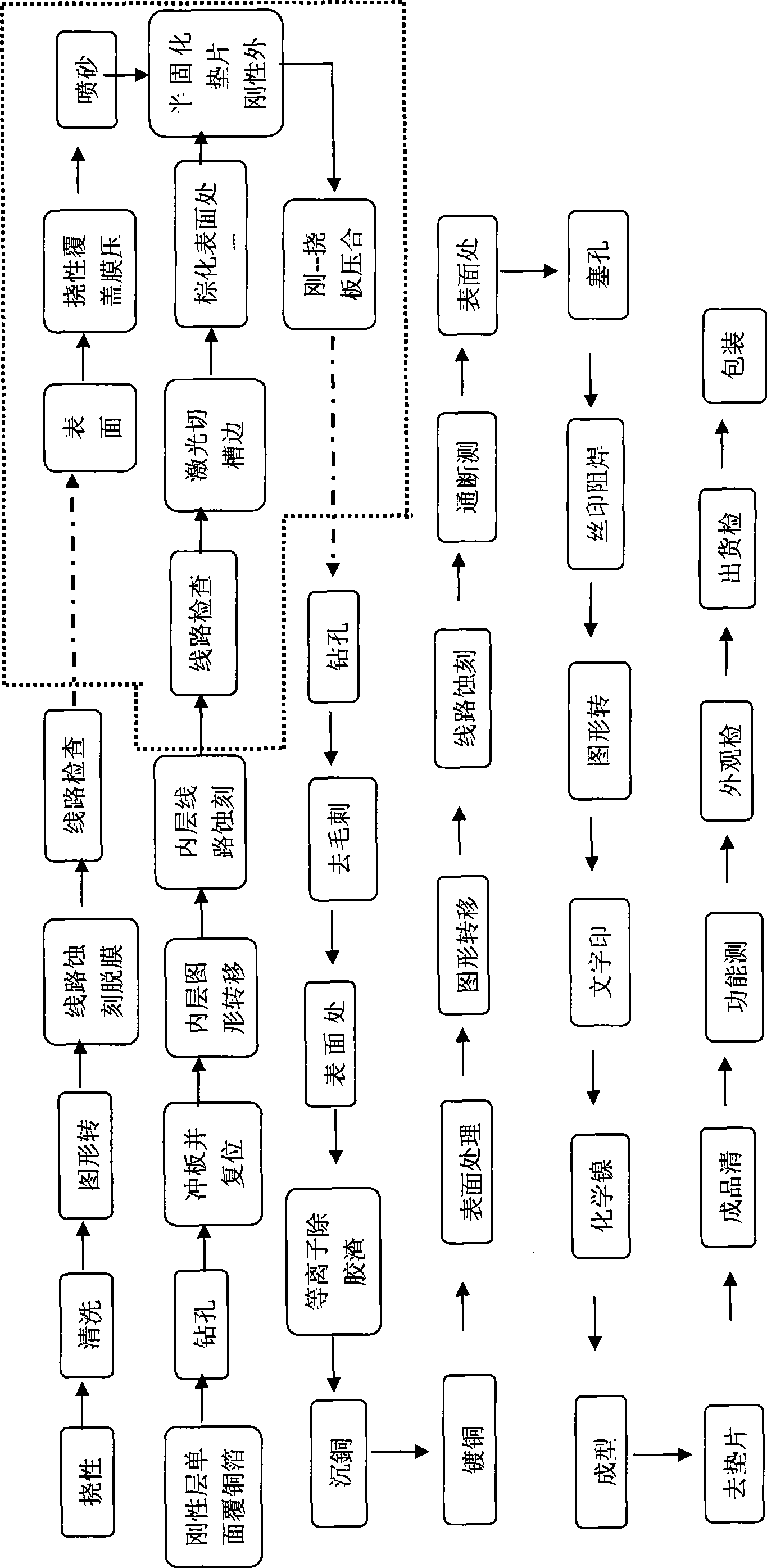
like figure 2 As shown, the disadvantages of using laser cutting groove edge are: (1) The price of laser equipment is high. A domestic equipment costs more than RMB 2.5 million, and its parts and maintenance costs are high. The equipment maintenance costs are higher and the maintenance period is long, resulting in high processing costs; (2) Since the rigid-flexible printed circuit board has a certain thickness, the cutting energy is easy to cause carbonization of the cutting position, and if the cutting energy is not well controlled, it will be damaged by carbon powder pollution. The formation of short circuits or black edges directly affects product quality; (3) If half-break or partial laser cutting is used, the efficiency is lower when the second laser cutting is performed during the shape forming, because the rigid-flexible printed circuit board has a certain Expansion and contraction, and it is also prone to interface inconsistency and misalignment

Method used


Image

  • Manufacturing method for multilayered rigidity and flexibility combined printed circuit board
  • Manufacturing method for multilayered rigidity and flexibility combined printed circuit board
  • Manufacturing method for multilayered rigidity and flexibility combined printed circuit board

Examples


Embodiment 1

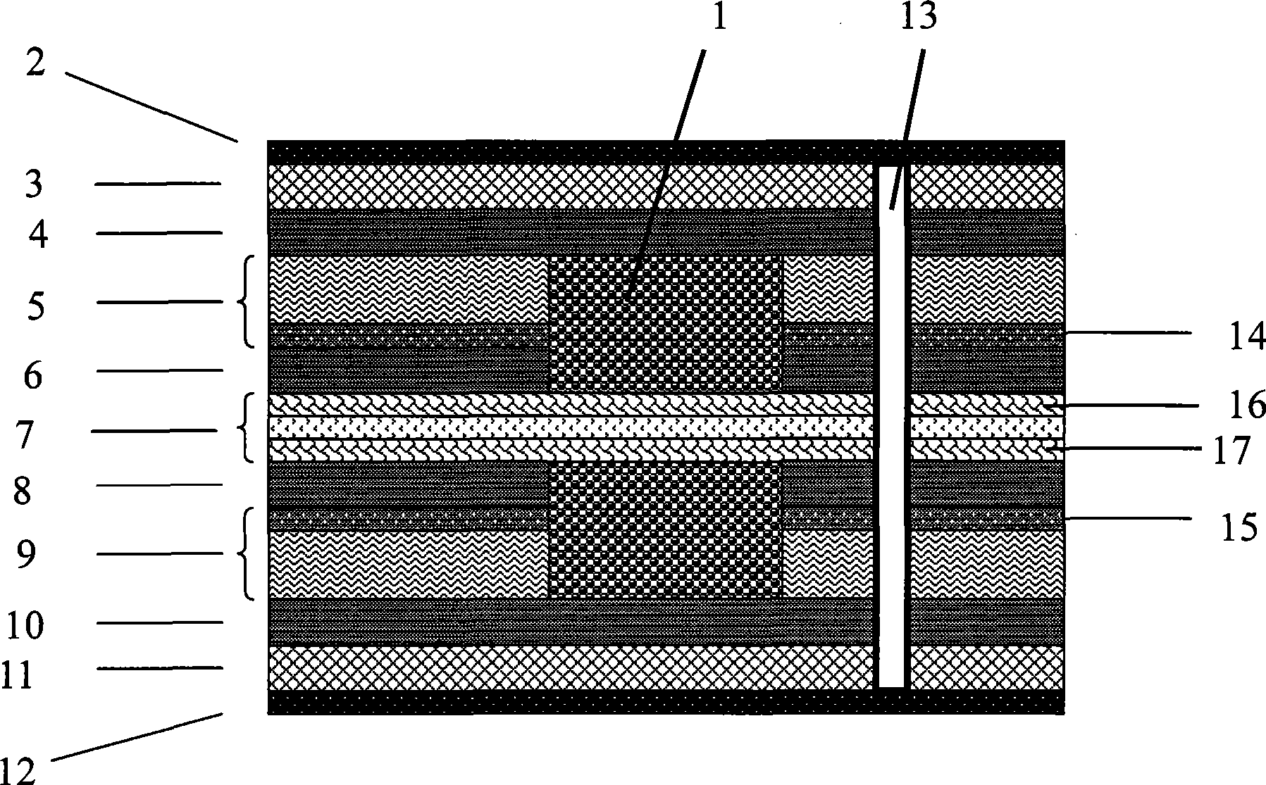
[0021] Embodiment 1, the making of six-layer rigid-flexible printed wiring board, such as image 3 As shown, the specifications are two-layer flexible circuit board FPC in the middle and two-layer rigid circuit board PCB on both sides. The rigid circuit board circuit is ≥0.1mm, and the board thickness is 1.5±0.03mm. The thickness of the film is 25um, and the pure copper foil is 18um. The area is 50mm×70mm.

[0022] The specific steps are: 1. First, according to the process steps of the prior art, the flexible circuit board 7 located in the middle is completely processed;

[0023] 2. After processing the inner single-sided copper foils of the rigid circuit boards 5 and 9 on both sides of the flexible circuit board 7 according to the prior art, use a drilling machine to drill the relevant positioning holes and auxiliary holes on the side close to the flexible circuit board 7. hole;

[0024] 3. Forging machine tools are used. Forging machine tools with a tonnage of 25 tons of p...


PUM


Abstract

The invention discloses a method for manufacturing multilayer flex-rigid printed circuit boards, and aims to solve the technical problem of filling efficiency and product quality in the process of processing the multilayer flex-rigid printed circuit boards. The method comprises that: preprocesses of a rigid circuit board part and a flexible circuit board part are carried out respectively, laminated and formatted, and then thermally compressed and overlapped, and a filler piece is processed by a punching method for the rigidity wiring board part; and when a rigid circuit board is processed, a rigid single-side copper-clad material is adopted, and then the following steps are completed in order: drilling, punching, transfer of inner layer patterns, etching of an inner layer circuit, circuit inspection, surface multibond, and semi-solid preparation of a rigid outer layer film of a washer and pure copper foil. Compared with the prior technology, hardware mould is directly used to perform die cutting on the filler piece on the position of a filling area; therefore, the method reduces the generation of bug dust in the processing process, has good leak tightness of the filling position, and greatly improves the reliability of performance and product percent of pass.

Description

technical field [0001] The invention relates to a method for manufacturing a printed circuit board, in particular to a method for manufacturing a rigid-flexible multilayer printed circuit board. Background technique [0002] In recent years, with the rapid growth of consumer electronics products, such as mobile phones, laptop computers, digital cameras, digital cameras, VCD, DVD, miniature tape recorders, pickups and fitness monitors, the printed circuit board PCB has been continuously developed to high density. , high precision, high reliability, large area, thin line and small aperture, resulting in a single rigid printed board or flexible printed board can no longer meet the requirements of miniaturization, light weight and multi-function of electronic products , So rigid-flexible printed circuit boards appeared. Rigid-Flex Printed Circuit Board (Rigid-Flex Printed Circuit Board), also known as rigid-flex board, referred to as R-FPCB, is selectively laminated by rigid an...

Claims


Application Information

Patent Timeline
IPC IPC(8): H05K3/46
Inventor 牛勇
Owner 吉安新宇腾跃电子有限公司
Learn More