Carbon nanowall with controlled structure and method for controlling carbon nanowall structure

A carbon nanowall and structure control technology, applied in the field of carbon nanowall, can solve the problems of non-interconnection and inferior substrate orientation

Inactive Publication Date: 2009-07-22
TOYOTA JIDOSHA KK
View PDF1 Cites 13 Cited by
  • Summary
  • Abstract
  • Description
  • Claims
  • Application Information

AI Technical Summary

Problems solved by technology

In addition, carbon nanoflakes are similar to carbon nanowalls with two-dimensional expansion of planar small pieces, but like rose petals, the small pieces are not connected to each other, and the orientation with respect to the substrate is inferior to that of carbon nanowalls. carbon nanostructure

Method used


Image

  • Carbon nanowall with controlled structure and method for controlling carbon nanowall structure
  • Carbon nanowall with controlled structure and method for controlling carbon nanowall structure
  • Carbon nanowall with controlled structure and method for controlling carbon nanowall structure

Examples


Embodiment 1

[0032] use figure 2 The plasma CVD apparatus shown, and the substrate 2 that is formed by silicon (Si) is arranged on the heater 3 in the chamber, introduces carbon source gas (C 2 f 6 ), while introducing hydrogen (H 2 ). At this time, the temperature of the heater 3 was set at 970°C.

[0033] The distance between the plate electrode 4 and the substrate 2 is set to 5 cm, and the electric output of the plasma generator 7 is 13.56 MHz and 100 W, so that capacitively coupled plasma is generated between the plate electrode 4 and the substrate 2 . In addition, inductively coupled plasma is generated in the introduction tube 6 by the inductive plasma generating source 8 . At this time, the output of the high-frequency output device 9 is 13.56 Hz and 400 W. The area of ​​the parallel plate electrodes is 19.625cm 2 (Φ50mm).

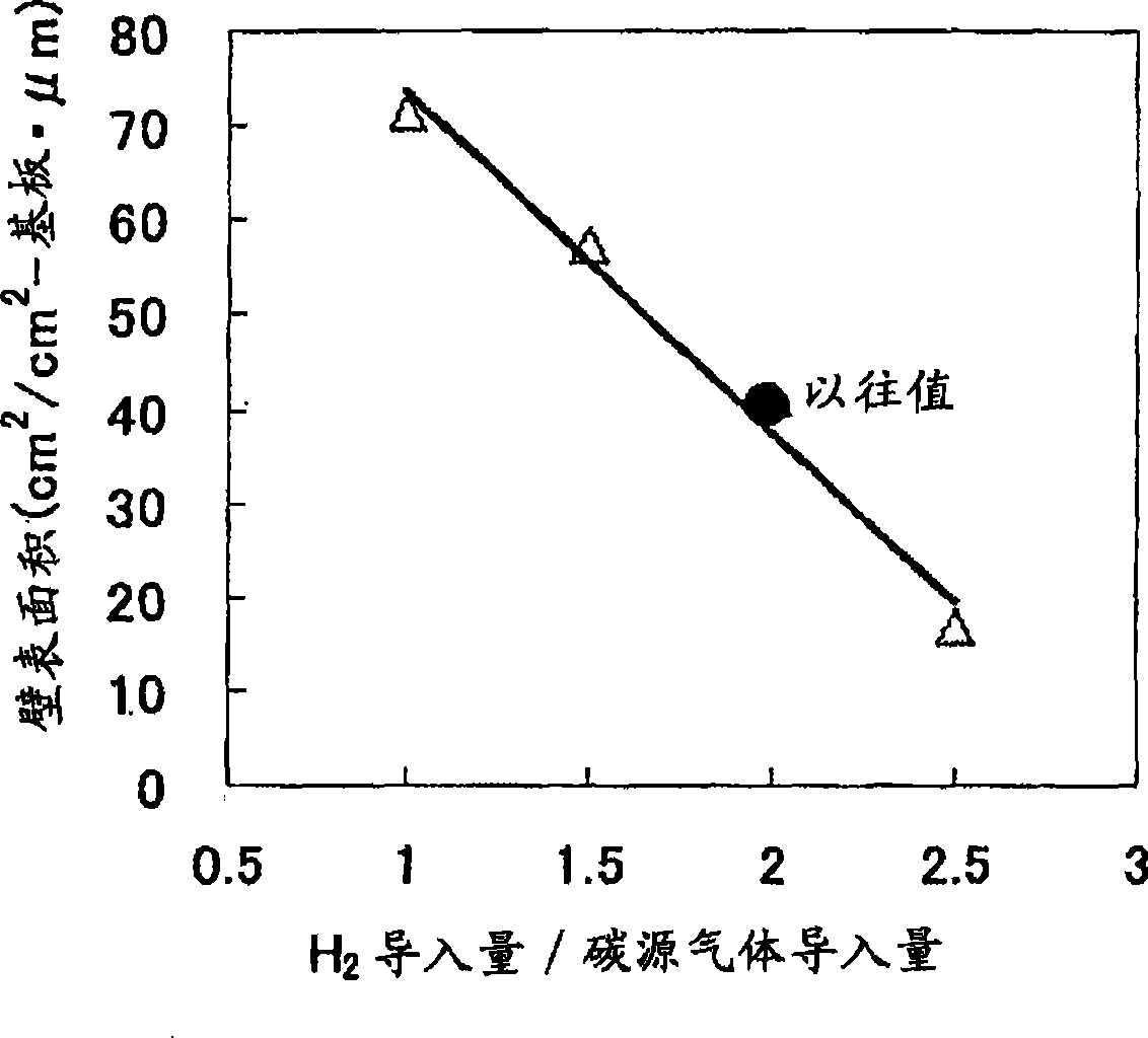
[0034] Carbon nanowalls (CNW) were grown on the substrate 2 by the plasma CVD method under the aforementioned conditions. The flow of carbon source gas...

Embodiment 2

[0039] It has been proved that in the same CVD process as in Example 1, by making H 2 It is also possible to independently control the crystallinity by varying the amount of gas introduced.

[0040] Figure 6 means H 2 The relationship between the amount of introduction and the crystallinity of the carbon nanowall determined by Raman spectroscopic analysis. The level of crystallinity was estimated using the half-value width of the D band of the Raman spectrum measured at an irradiation laser wavelength of 514.5 nm as an index. The smaller the half-value width of the D band, the higher the crystallinity. That is, by reducing H 2 The introduction amount can improve the crystallinity of the carbon nanowall. exist Figure 6 In , for reference, the D-band half-value width of Ketjen black (Ketjenblack) and the D-band half-value width of graphite, which are conventional carriers, are added. It can be seen that even carbon nanowalls can obtain high crystallinity higher than Ket...


PUM

PropertyMeasurementUnit
areaaaaaaaaaaa

Abstract

The invention provides a method of controlling the structure of carbon nanowall (CNW) in which the interwall spacing of carbon nanowall (CNW) is varied so as to control the surface area thereof or control the crystallinity thereof, thereby enhancing the corrosion resistance at high potential; and a highly crystalline carbon nanowall (CNW) and carbon nanowall (CNW) of large surface area with controlled structure. There are provided (1) carbon nanowall characterized by having a wall surface area of 50 cm / cm-substrate mum or greater, (2) carbon nanowall characterized by having a crystallinity such that the D-band half value width of Raman spectrum measured with an irradiation laser wavelength of 514.5 nm is 85 cm or less; and (3) carbon nanowall characterized by having not only a wall surface area of 50 cm / cm-substrate mum or greater but also a crystallinity such that the D-band half value width of Raman spectrum measured with an irradiation laser wavelength of 514.5 nm is 85 cm or less.

Description

technical field [0001] The present invention relates to a method for controlling the structure of carbon nanowalls, and at the same time relates to a novel carbon nanowall whose structures such as surface area and crystallinity obtained by the method are controlled. Background technique [0002] Carbon-based porous materials having a nanoscale structure include graphite and amorphous carbon-based porous materials, for example, known fullerenes, carbon nanotubes, carbon nanohorns, and carbon nanoflakes. [0003] Among carbon-based porous materials with a nanoscale structure, a carbon nanowall (CNW) is a carbon nanostructure that expands two-dimensionally, and a typical example is a wall-like structure that rises from the surface of the substrate in a substantially constant direction. carbon nanowalls. Fullerenes (C60, etc.) are zero-dimensional carbon nanostructures, and carbon nanotubes can be regarded as one-dimensional carbon nanostructures. In addition, carbon nanoflake...

Claims


Application Information

Patent Timeline
Patent Type & Authority Applications(China)
IPC IPC(8): C01B31/02B01J32/00B01J21/18H01M4/96
CPCH01M4/9083B01J21/185H01M4/926C01B31/0293Y02E60/50B82Y40/00B82Y30/00C01B32/18Y10T428/24355
Inventor 堀胜平松美根男加纳浩之杉山彻滨雄一郎
Owner TOYOTA JIDOSHA KK
Why Eureka
Try Eureka