
Connection pore forming method

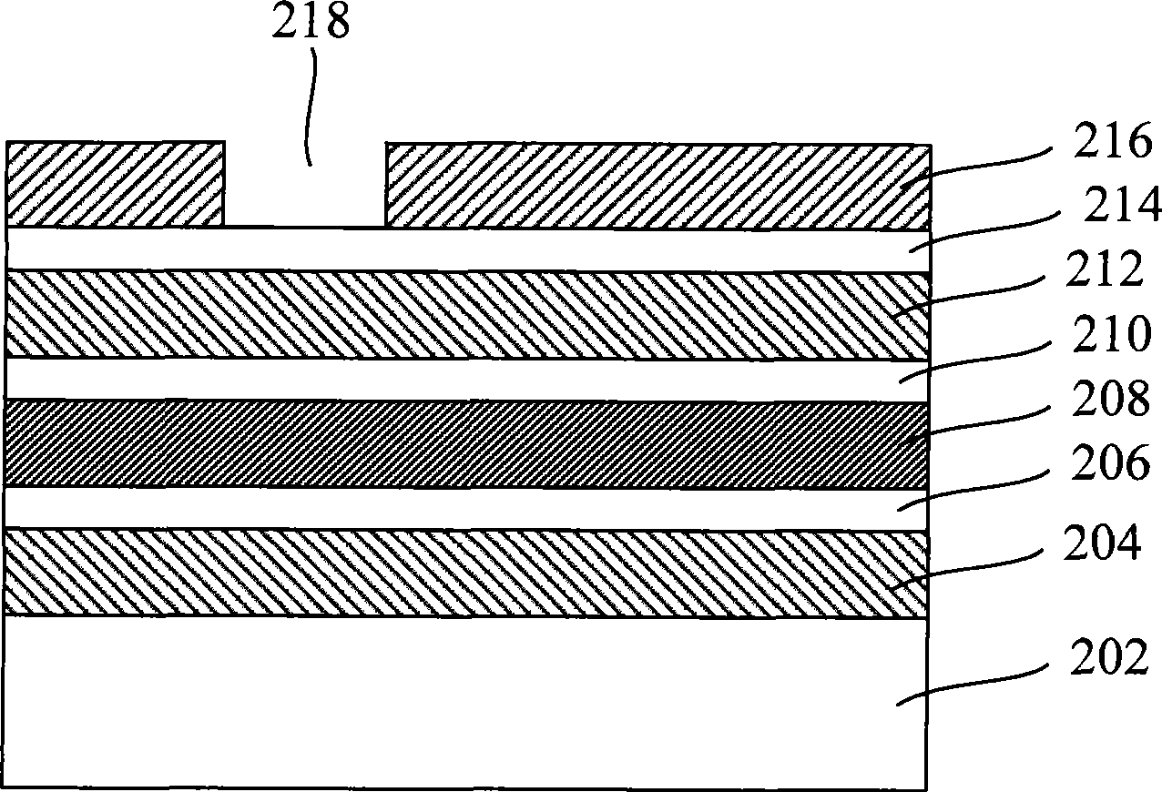
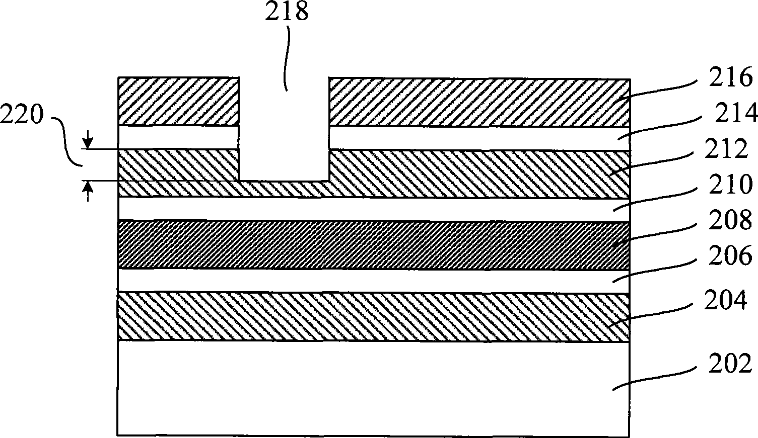
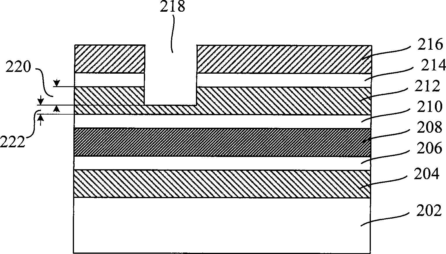
A connection hole and process technology, which is applied in the field of connection hole formation, can solve problems such as incomplete removal of the organic glass layer 212, affecting the conductivity of semiconductor devices, and the connection hole is not opened.

Active Publication Date: 2009-06-17
SEMICON MFG INT (SHANGHAI) CORP
View PDF1 Cites 20 Cited by
  • Summary
  • Abstract
  • Description
  • Claims
  • Application Information

AI Technical Summary

Problems solved by technology

However, with the development of the semiconductor manufacturing process to high-tech nodes, such as 65nm or even 45nm, the line width of the connection hole is getting smaller and smaller, and the existing etching method can no longer meet the needs of high-tech nodes. , it is easy to cause the problem of incomplete removal of the plexiglass layer 212, thereby easily causing defects such as the bottom of the formed connection hole not being opened (Via Open), which affects the conductivity of the formed semiconductor device

Method used


Image

  • Connection pore forming method
  • Connection pore forming method
  • Connection pore forming method

Examples


Embodiment Construction

[0059] The specific embodiments of the present invention will be described in detail below in conjunction with the accompanying drawings.

[0060] In the manufacturing process of the dual damascene structure, the connection hole (Via First) can be formed in the intermetal dielectric layer first, and then the trench can be formed; the trench (Trench First) can also be formed first, and then the connection hole can be formed; The holes and trenches are filled with metal material, forming a dual damascene structure.

[0061] The invention provides a method for manufacturing connection holes, which can be applied to the manufacture of connection holes in the manufacturing process of forming connection holes first and then forming grooves in the dual damascene structure, and is also suitable for forming grooves first and then forming connection holes. Fabrication of connection holes in the manufacturing process of the hole dual damascene structure.

[0062] Figure 4 It is a flow...


PUM

PropertyMeasurementUnit
thicknessaaaaaaaaaa
thicknessaaaaaaaaaa

Abstract

A method of forming connecting holes comprises steps of providing a semiconductor structure with an etch stop layer, wherein the etch stop layer is equipped with an intermetallic dielectric layer, forming a photoresist layer on the intermetallic dielectric layer, patterning the photoresist layer to form a connecting hole pattern, executing the major etching process to etch part of thickness of the intermetallic dielectric layer at the bottom portion of the connecting hole pattern, after the major etching process is finished, executing the first step of the over-etching process to etch residual thickness of the intermetallic dielectric layer and form an opening in the intermetallic dielectric layer, wherein the bottom of the opening exposes out of the etch stop layer, then executing the second step of the over-etching process to etch the bottom of the opening, and finally removing the etch stop layer at the bottom of the opening. The invention can avoid the defect that the bottom of the connecting hole is not opened.

Description

technical field [0001] The invention relates to the technical field of semiconductor manufacturing, in particular to a method for forming a connection hole (Via). Background technique [0002] With the continuous development of semiconductor integrated circuit manufacturing technology, the line width of semiconductor devices is getting smaller and smaller. In order to reduce the resistance and capacitance delay (RC Delay) of the back-end metal interconnection structure, the industry uses copper as the interconnection metal and low dielectric The constant material is used as the dielectric material between the interconnect lines, and a dual damascene process is used to manufacture copper and low dielectric constant dual damascene structures. [0003] The manufacturing process of the dual damascene structure is generally as follows: firstly, an intermetallic dielectric layer is formed, and the intermetallic dielectric layer is a low dielectric constant material; then, connecti...

Claims


Application Information

Patent Timeline
Patent Type & Authority Applications(China)
IPC IPC(8): H01L21/768H01L21/311
Inventor 孙武沈满华王新鹏
Owner SEMICON MFG INT (SHANGHAI) CORP
Learn More