
LED structure and manufacturing method thereof

A technology of light-emitting diodes and manufacturing methods, which is applied in the direction of electrical components, circuits, semiconductor devices, etc., can solve the problems of cumbersome and time-consuming, increase costs, and do not meet the commercial application of light-emitting diodes, so as to reduce the probability of total reflection, make it simple, Effect of improving light extraction rate

Inactive Publication Date: 2009-04-22
TEKCORE CO LTD
View PDF1 Cites 15 Cited by
  • Summary
  • Abstract
  • Description
  • Claims
  • Application Information

AI Technical Summary

Problems solved by technology

This kind of manufacturing process is not only cumbersome and time-consuming, but also increases a lot of cost, which is not suitable for the commercial application of light-emitting diodes.

Method used


Image

  • LED structure and manufacturing method thereof
  • LED structure and manufacturing method thereof
  • LED structure and manufacturing method thereof

Examples


Embodiment Construction

[0019] The detailed content and technical description of the present invention will be further described by examples, but it should be understood that these examples are for illustrative purposes only, and should not be construed as limitations on the implementation of the present invention.

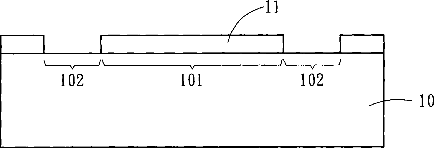
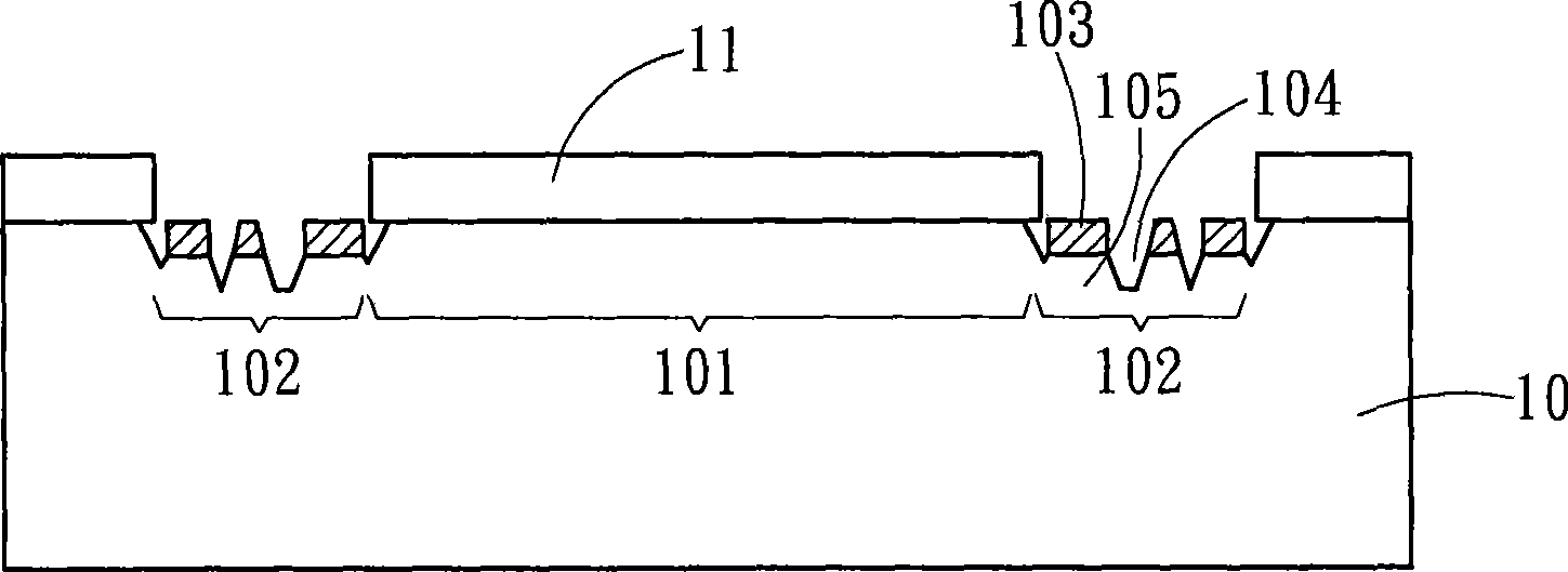
[0020] see Figure 1 to Figure 5 shown. The manufacturing method of the light-emitting diode of the present invention includes: first, providing the substrate 10, and the substrate 10 is one of sapphire, silicon carbide, silicon, gallium arsenide, aluminum nitride, and gallium nitride substrates. A passivation layer 11 is grown on the surface of the substrate 10, and the passivation layer 11 is patterned to define the element area 101 covered by the passivation layer 11 and the scribe area 102 exposed on the surface of the substrate 10 (such as figure 1 shown).

[0021] Then, the substrate 10 is placed in the first solution to react, so that the surface of the substrate 10 exposed from...


PUM


Abstract

The invention discloses an LED structure and a fabrication method. The method comprises the following steps: placing a substrate in a solution for reaction; naturally forming a chemical reaction layer on the surface of a cutting street region of the substrate; forming a plurality of concave parts and convex parts on the surface of the cutting street region by selective etching; growing a semiconductor layer structure on a component region and the cutting street region on the surface of the substrate by an epitaxial growth technology; and then forming the LED by the semiconductor layer structure on the component region using yellow light lithography process.

Description

technical field [0001] The present invention relates to a light emitting diode structure and a manufacturing method, in particular to a light emitting diode structure and a manufacturing method in which a plurality of concave parts and convex parts are formed on the surface of the cutting line area. Background technique [0002] In order to realize solid-state lighting, it is imperative to develop and improve the luminous efficiency of light-emitting diodes. The ways to improve the luminous efficiency of LEDs can be divided into two parts: one is to improve the internal quantum efficiency of LEDs; the other is to increase the external quantum efficiency (light extraction rate) of LEDs. [0003] In terms of external quantum efficiency, because the refractive index of the general semiconductor material and the packaging material is very different, the total reflection angle is small, so when the light generated by the light-emitting diode reaches the interface with the air, th...

Claims


Application Information

Patent Timeline
Patent Type & Authority Applications(China)
IPC IPC(8): H01L33/00H01L33/20
Inventor 林宏诚李家铭綦振瀛
Owner TEKCORE CO LTD
Learn More