Passivation encapsulation method for back electrode of solar cell
A technology for solar cells and packaging methods, applied in the fields of circuits, electrical components, sustainable manufacturing/processing, etc., can solve problems such as affecting electrical properties and affecting the efficiency of amorphous silicon solar cells
- Summary
- Abstract
- Description
- Claims
- Application Information
AI Technical Summary
Problems solved by technology
Method used
Image
Examples
Embodiment 1
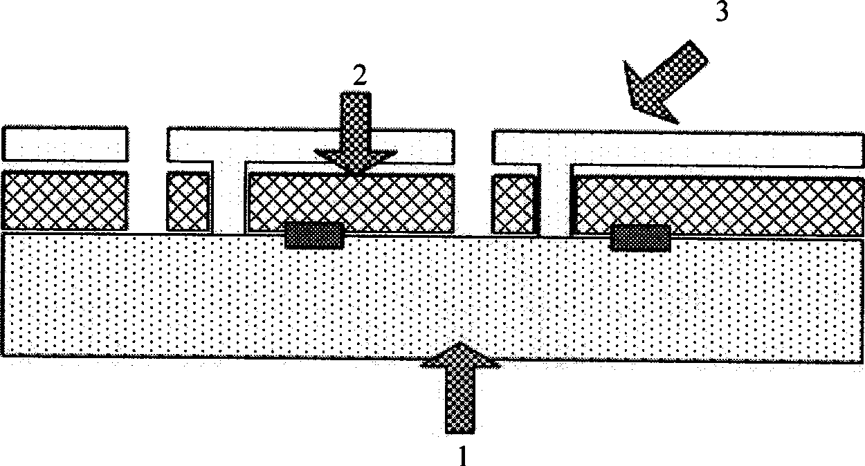
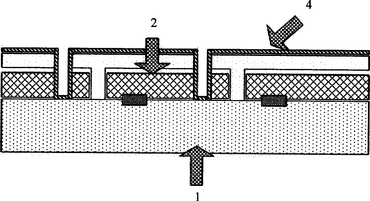
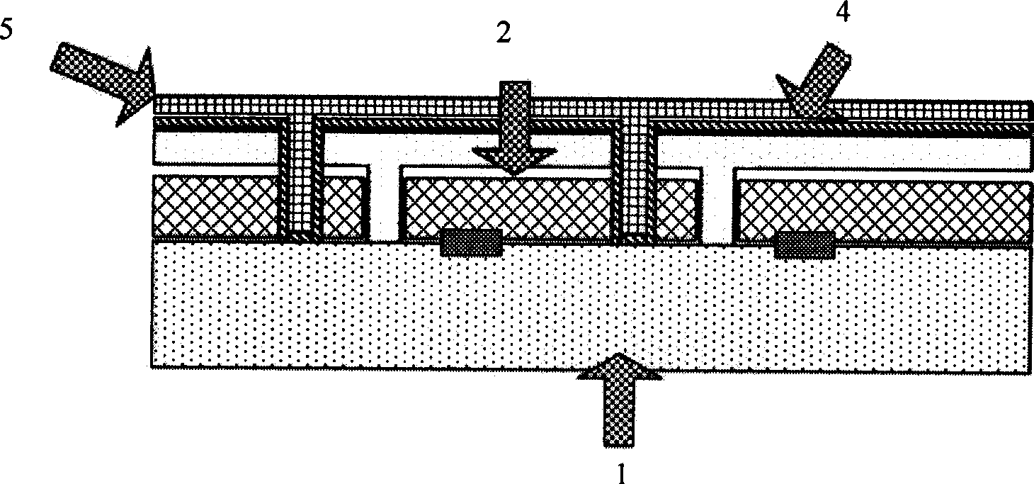
[0035] Aluminum oxide and silicon dioxide thin films are used as passivation encapsulation layers, and are sputtered on the back of the metal interconnection layer 3 by magnetron sputtering. The cell is placed in a chamber of magnetron sputtering, and the target material is an aluminum oxide target. The etched back electrode is sputtered in the chamber to cover and passivate the etched area to form a dense protective layer.
[0036] Alternatively, the aluminum electrodes of the reflective layer and the conductive layer are plated first, and then etched with a laser, and the cell is placed in the magnetron sputtering chamber, and the target material is a silicon dioxide target. It is sputtered to coat and passivate the etched place to form a dense silicon dioxide protective layer.
Embodiment 2
[0038] Aluminum oxide and silicon dioxide thin films are used as passivation encapsulation layers, and are deposited on the back of the metal interconnection layer 3 by using plasma enhanced chemical vapor deposition (PECVD).
[0039] Use PECVD to deposit silicon dioxide process: perform silane (SiH 4 ) and oxygen reaction, the reaction temperature is between 200 and 500°C, and the silicon dioxide film is deposited and grown. This method is simple and can easily deposit a passivation film on the back electrode.
[0040] Use PECVD to deposit aluminum oxide: react organic aluminum source and oxygen on the back of the metal interconnection layer 3 at a reaction temperature of 200-500° C. to deposit and grow aluminum oxide passivation film. The organic aluminum source can be triethylaluminum (Al(CH 2 CH 3 ) 3 ), triisobutylaluminum, etc.
Embodiment 3
[0042] Polyimide is used as a passivation encapsulation layer, and is coated, sprayed, or spin-coated on the back of the metal interconnection layer 3 .
[0043] The polyamic acid solution is coated to form a film, and then cured by heating at a temperature below 300°C to convert the polyamic acid into polyimide. At the same time, it has the advantage of simple process, only two steps are required: apply the coating glue directly on the back of the metal interconnection layer 3, and send it to an oven for heating and curing; no need to add any catalyst, curing agent and other additives.
PUM
| Property | Measurement | Unit |
|---|---|---|
| Thickness | aaaaa | aaaaa |
Abstract
Description
Claims
Application Information
 - R&D
- Intellectual Property
- Life Sciences
- Materials
- Tech Scout
- Unparalleled Data Quality
- Higher Quality Content
- 60% Fewer Hallucinations
Browse by: Latest US Patents, China's latest patents, Technical Efficacy Thesaurus, Application Domain, Technology Topic, Popular Technical Reports.
© 2025 PatSnap. All rights reserved.Legal|Privacy policy|Modern Slavery Act Transparency Statement|Sitemap|About US| Contact US: help@patsnap.com


