LED chip / wafer/ epitaxial slice non-contact type checking method and checking device
A technology of LED chips and detection methods, which is applied in the direction of measuring devices, semiconductor/solid-state device testing/measurement, photometry, etc., can solve problems such as damage, increased production costs, and difficulty in adoption, and achieve the effect of reducing costs
- Summary
- Abstract
- Description
- Claims
- Application Information
AI Technical Summary
Problems solved by technology
Method used
Image
Examples
Embodiment 1
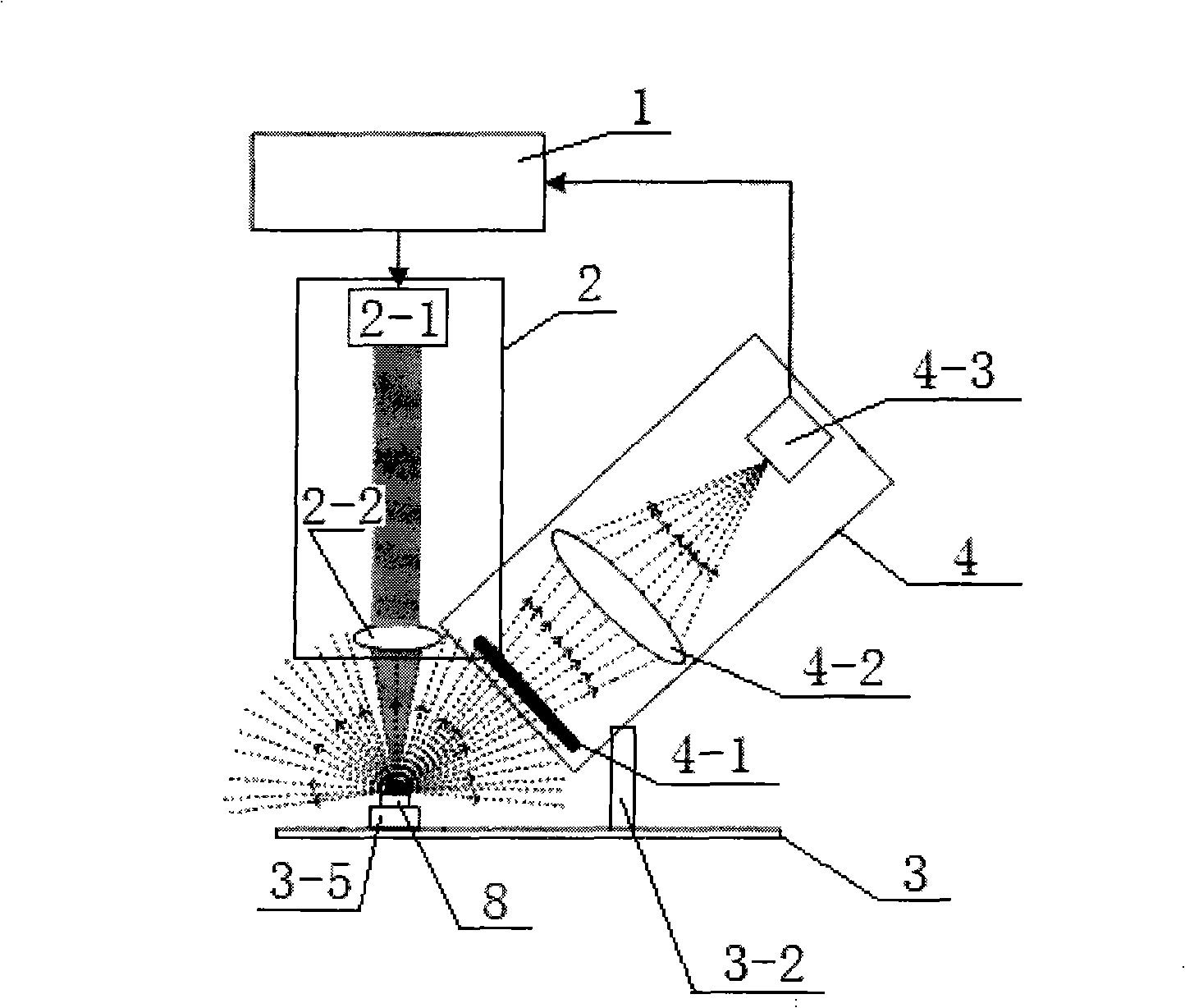
[0074] See attached figure 1 , the detection device includes: a detection control and signal processing unit 1, a light source unit 2, a test bench 3, and a light detection unit 4, wherein the detection control and signal processing unit 1 controls the light source unit 2 to emit excitation light and transmits excitation light to the light detection unit 4 The incoming signal is processed and analyzed, the optical detection unit 4 collects the optical signal and transmits it to the detection control and signal processing unit 1 , and the test bench 3 is used to clamp / move the device under test 8 and support the optical detection unit 4 .
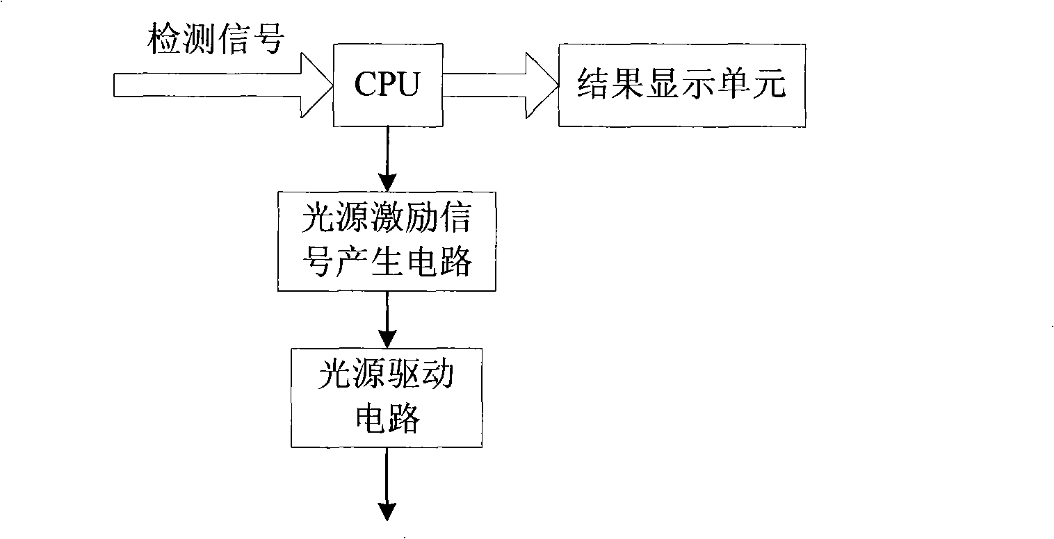
[0075] See attached figure 2 , wherein the detection control and signal processing unit 1 includes: a CPU, a result display unit, a light source excitation signal generation circuit, and a light source drive circuit, wherein the input end of the CPU is connected to the output end of the light detection unit 4 in communication, and the outpu...
Embodiment 2
[0080] See attached Figure 4 , the test bench 3 includes: platform 3-1, supporting device 3-2, guide rail 3-3, transmission device 3-4, clamping 3-5, stepper motor 1 3-6, wherein, guide rail 3-3, The clamp 3-5 is fixed on the platform 3-1, the clamp 3-5 is used to clamp the device 8 to be tested, the support device 3-2 is fixed on the transmission device 1 3-4 and is mechanically connected with the light detection unit 4, Stepping motor one 3-6 drives transmission device 3-4 to slide on guide rail 3-3.
[0081] Embodiment 2 is different from Embodiment 1 in that: in order to detect self-illumination from different directions, the light detection unit 4 is connected with the transmission device 1 3-4 through the supporting device 3-2, and is placed on the guide rail 3-3 to detect The control and signal analysis and processing unit 1 controls the stepper motor 3-6 to drive the transmission device 3-4 to move along the guide rail 3-3, so that the light detection unit 4 also mov...
Embodiment 3
[0084] see Figure 7, the test platform 3 is also fixedly connected with a scanning platform 5, and the scanning platform 5 is externally connected with a stepping motor 2 6 and a transmission device 2 7, wherein the stepping motor 2 6 drives the transmission device 2 7, and the transmission device 2 7 drives the scanning platform 5 Moving, the scanning table 5 drives the test table 3 to move, so that the position between the clamping 3-5 and the test table 3 can be relatively static or moving, which is used for the detection of the LED array on the LED wafer / epitaxial wafer.
[0085] This example differs from Embodiments 1 and 2 in that: the test platform 3 is fixed on the scanning platform 5, and the detection control and signal analysis and processing unit 1 controls the stepping motor 2 6 to drive the scanning platform 5 to move through the transmission device 2 7 to realize Scanning inspection of LED arrays on epitaxial wafers / wafers.
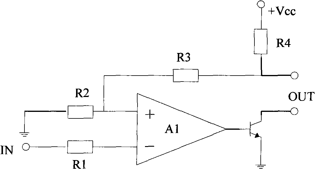
[0086] see Figure 8 , the signal...
PUM
 Abstract
Description
Claims
Application Information
 - R&D
- Intellectual Property
- Life Sciences
- Materials
- Tech Scout
- Unparalleled Data Quality
- Higher Quality Content
- 60% Fewer Hallucinations
Browse by: Latest US Patents, China's latest patents, Technical Efficacy Thesaurus, Application Domain, Technology Topic, Popular Technical Reports.
© 2025 PatSnap. All rights reserved.Legal|Privacy policy|Modern Slavery Act Transparency Statement|Sitemap|About US| Contact US: help@patsnap.com


