Manufacturing method for embedding heat radiating fin on printed circuit board
A printed circuit board and manufacturing method technology, applied in the directions of printed circuit manufacturing, printed circuit, multilayer circuit manufacturing, etc., can solve the problems of difficult processing, metal offset, abnormal grinding plate, etc. Concave or protruding, reduce abnormal wear, good effect of embedment
- Summary
- Abstract
- Description
- Claims
- Application Information
AI Technical Summary
Problems solved by technology
Method used
Image
Examples
Embodiment 1
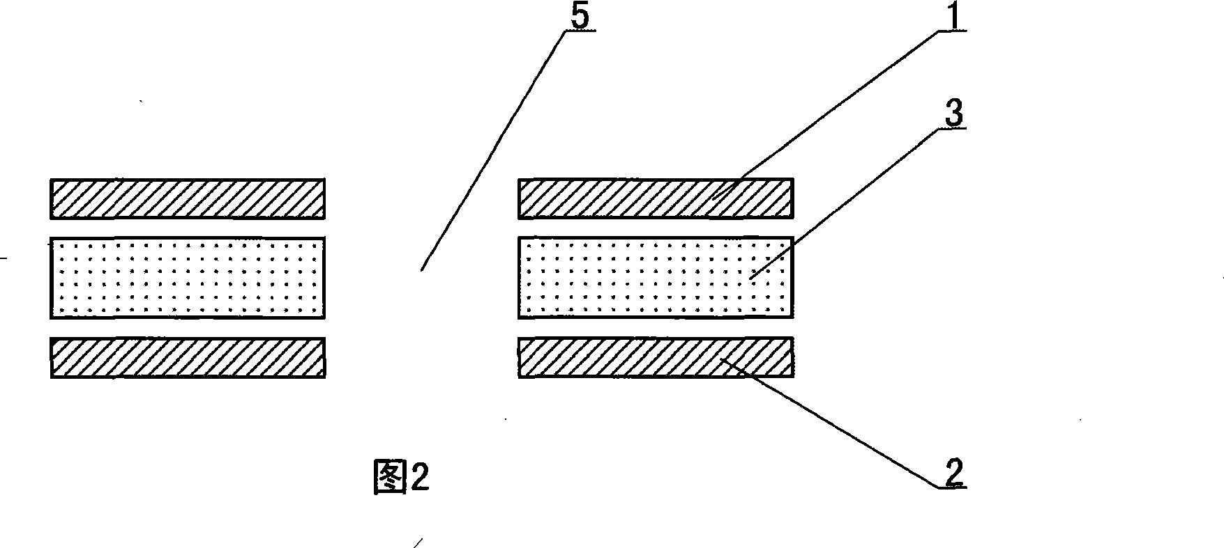
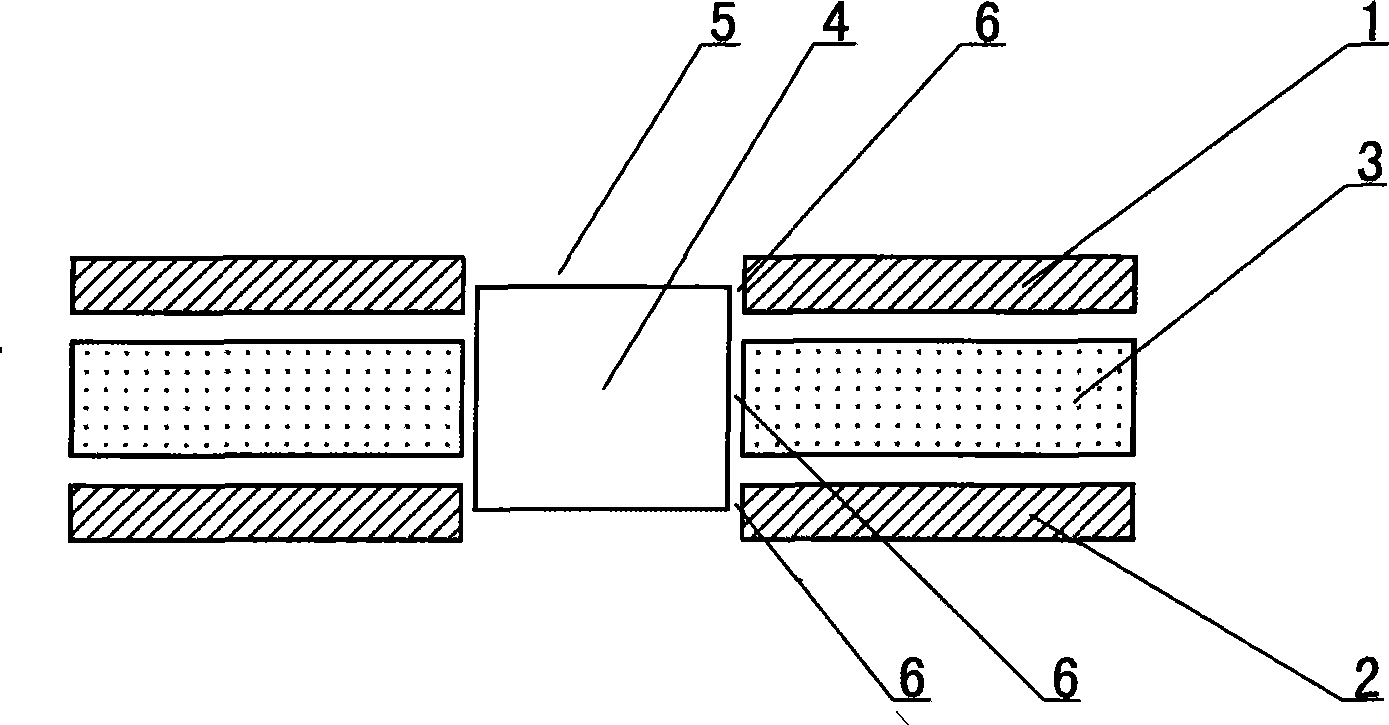
[0031] like Figure 1 to Figure 4 As shown, a manufacturing method for embedding a heat sink on a printed circuit board includes the following steps:
[0032] 1) In the molding area 12 of the first circuit board 1, the prepreg 3 and the second circuit board 2 ( figure 1 Open the tool hole 5 at the position of the pre-embedded heat sink 4 in the area in the middle solid line), and at the same time, outside the molding area 12 of the first circuit board 1, the prepreg 3 and the second circuit board 2 ( figure 1 The region between the solid line and the dotted line) drills the pre-alignment hole 10;
[0033] The above-mentioned first circuit board 1 and second circuit board 2 are multilayer circuit boards, wherein there are at least two conductive layers and a conductive signal layer;
[0034] Above-mentioned tool hole 5 can adopt the mechanical processing of modes such as punching or drilling;
[0035] The above-mentioned prepreg 3 adopts a prepreg with a resin content of 63%...
Embodiment 2
[0043] like Figure 5 to Figure 8 As shown, embodiment 2 is a manufacturing method for embedding heat sinks on a printed circuit board with three circuit layers, comprising the following steps:
[0044] 1) Open the tool hole 5 at the position of the pre-embedded heat sink 4 in the molding area 12 of the first circuit board 1, the first prepreg 3, the second circuit board 2, the second prepreg 7 and the third circuit board 8, and at the same time, The first circuit board 1, the first prepreg 3, the second circuit board 2, the second prepreg 7 and the molding area 12 of the third circuit board 8 are drilled with pre-alignment holes 10;
[0045] The above-mentioned first circuit board 1, second circuit board 2 and third circuit board 8 are multilayer circuit boards, wherein there are at least two conductive layers and conductive signal layers;
[0046] Above-mentioned tool hole 5 can adopt the mechanical processing of modes such as punching or drilling;
[0047] Both the first ...
PUM
 Abstract
Description
Claims
Application Information
 - R&D
- Intellectual Property
- Life Sciences
- Materials
- Tech Scout
- Unparalleled Data Quality
- Higher Quality Content
- 60% Fewer Hallucinations
Browse by: Latest US Patents, China's latest patents, Technical Efficacy Thesaurus, Application Domain, Technology Topic, Popular Technical Reports.
© 2025 PatSnap. All rights reserved.Legal|Privacy policy|Modern Slavery Act Transparency Statement|Sitemap|About US| Contact US: help@patsnap.com


