
Integrated circuit encapsulation structure for improving glue padding

An integrated circuit and filling technology, applied in the direction of circuits, electrical components, electrical solid devices, etc., can solve the problems of general products without structure, air bubbles 131 attached, and air covered, so as to facilitate the thinning of packaging and reduce the Air bubbles and crevices are formed to increase fluidity

Inactive Publication Date: 2008-08-13
CHIPMOS TECH INC
View PDF0 Cites 6 Cited by
  • Summary
  • Abstract
  • Description
  • Claims
  • Application Information

AI Technical Summary

Problems solved by technology

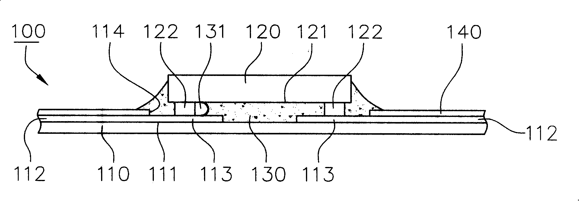
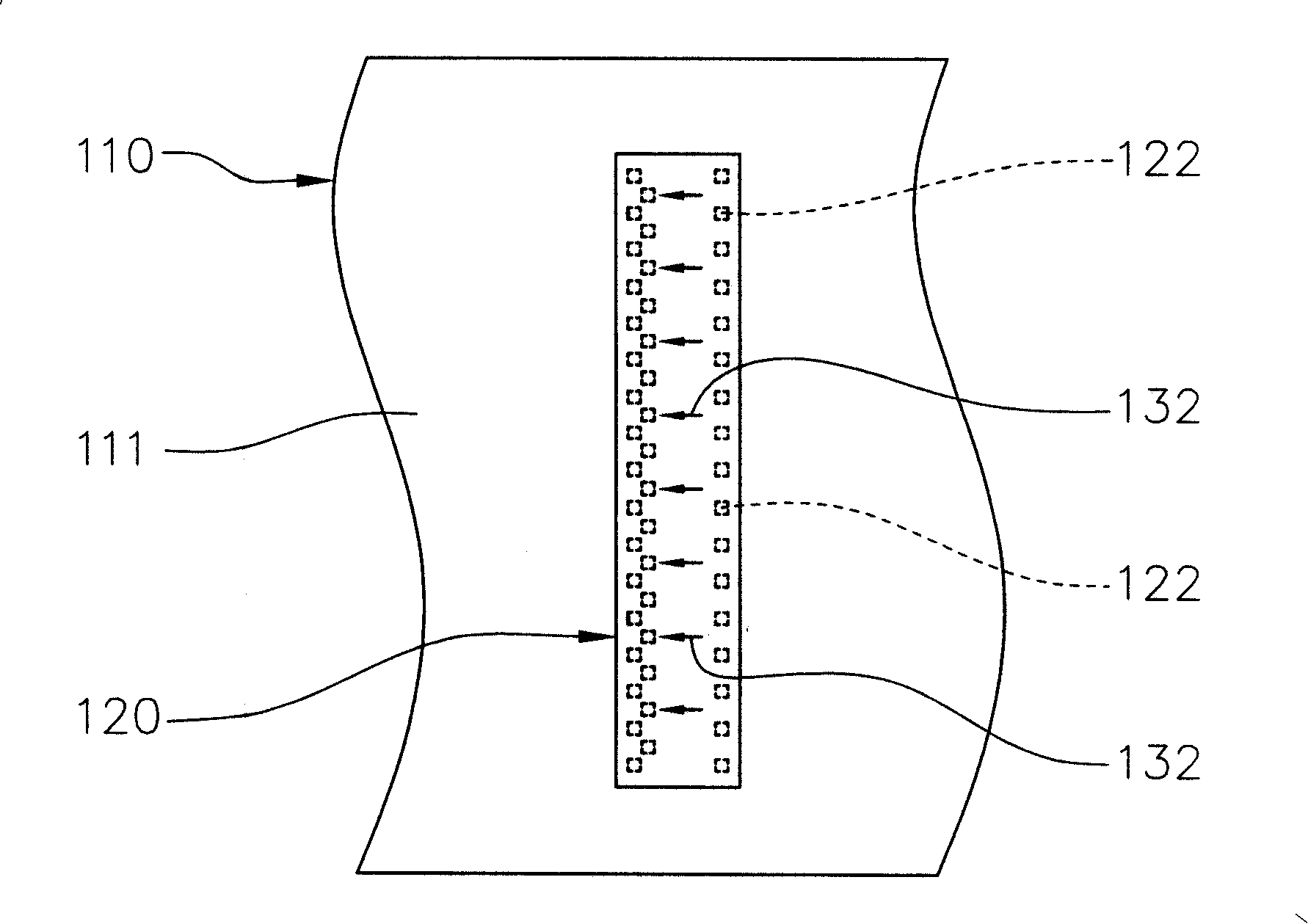
The liquid encapsulation resin 130 gradually covers the chip bonding area 114 of the substrate 110 and the periphery of the chip 120 according to the flow direction 132 of the glue. Since the viscosity of the liquid encapsulation resin 130 will limit its fluidity, it is easy to produce air encapsulation. phenomenon, so there is a problem that air bubbles 131 adhere to pins 112
[0004] It can be seen that the above-mentioned existing integrated circuit packaging structure obviously still has inconvenience and defects in structure and use, and needs to be further improved urgently.
In order to solve the above-mentioned problems, the relevant manufacturers have tried their best to find a solution, but no suitable design has been developed for a long time, and the general products do not have a suitable structure to solve the above-mentioned problems. This is obviously related. The problem that the industry is eager to solve

Method used


Image

  • Integrated circuit encapsulation structure for improving glue padding
  • Integrated circuit encapsulation structure for improving glue padding
  • Integrated circuit encapsulation structure for improving glue padding

Examples


Embodiment Construction

[0041] In order to further explain the technical means and effects of the present invention to achieve the intended purpose of the invention, below in conjunction with the accompanying drawings and preferred embodiments, the specific implementation and structure of the integrated circuit packaging structure for improving the filling property of the present invention are presented. , features and their effects are described in detail below.

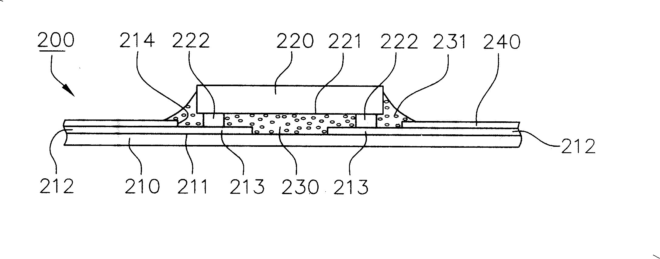
[0042] see image 3Shown is a schematic cross-sectional view of an integrated circuit package structure for improving the filling property according to a specific embodiment of the present invention. A specific embodiment of the present invention discloses an integrated circuit packaging structure that improves the filling property of the glue. The integrated circuit packaging structure 200 mainly includes a substrate 210 , a chip 220 and a highly filling liquid packaging resin 230 .

[0043] The substrate 210 has an upper surface 211 , ...


PUM


Abstract

The invention relates to an integrated circuit package structure that promotes the gluey fallibility, which comprises: a base plate and a wafer arranging on the base plate and electrically connecting to the base plate with a plurality of projections; and a fallibility liquid package resin forming between the base plate and the wafer for sealing these projections, wherein the fallibility liquid package resin comprises liquid crystal substance for promoting the gluey fallibility. The base plate of the invention may be one chip on flex film carrier which is favorable to encapsulation thinization, lightweight and flexibility; it provides appropriate package protection in order to prevent that electrical short circuit and dust pollution, and the fallibility liquid package resin comprises liquid crystal substance for promoting the gluey fallibility and reducing the form of bubble and gap; the liquid crystal substance may have ultraviolet ray (UV) solidifiability and avoid the electrical abnormity; the base plate of the integrated circuit package structure may otherwise comprises one solder mask which forms on the base plate and partially cover these pins and can avoid the short circuit caused by the pollution because of the exposure of the pins.

Description

technical field [0001] The invention relates to an integrated circuit packaging structure using liquid packaging resin, in particular to an integrated circuit packaging structure that improves the fillability of the glue, so as to eliminate air bubbles in the sealant. Background technique [0002] The known chip-on-film package (Chip-On-Film package, COF) has been a common integrated circuit packaging type, which is to apply liquid packaging resin on the chip that has completed the bonding of the chip and the substrate. Around, the gap between the wafer and the substrate is filled by capillary phenomenon. However, the liquid encapsulation resin often causes air bubbles to adhere to the pins for the fine-pitch high-pin-count integrated circuit design, especially if the chip is provided with two or more rows of bumps on one side. [0003] see figure 1 and figure 2 Shown is a schematic cross-sectional view of a conventional integrated circuit package structure and a schemat...

Claims


Application Information

Patent Timeline
Patent Type & Authority Applications(China)
IPC IPC(8): H01L23/29H01L23/488
CPCH01L2224/73204H01L2224/16225
Inventor 郭秀湲卢东宝
Owner CHIPMOS TECH INC
Learn More