
Semiconductor encapsulation structure for improving wafer shift upon pressing

A semiconductor and chip technology, applied in the field of lead frame, to protect the chip and improve the effect of vertical position deviation

Inactive Publication Date: 2009-05-20
CHIPMOS TECH INC
View PDF7 Cites 0 Cited by
  • Summary
  • Abstract
  • Description
  • Claims
  • Application Information

AI Technical Summary

Problems solved by technology

[0008] The main purpose of the present invention is to overcome the defects of the existing semiconductor package structure, and provide a new semiconductor package structure and the lead frame used to improve the displacement of the wafer during compression molding. The technical problem to be solved is to make it possible Provide sufficient length of these inclined pins to disperse the vertical mold flow pressure difference, and can improve the problem of wafer vertical position deviation during compression molding, which is very suitable for practical use

Method used


Image

  • Semiconductor encapsulation structure for improving wafer shift upon pressing
  • Semiconductor encapsulation structure for improving wafer shift upon pressing
  • Semiconductor encapsulation structure for improving wafer shift upon pressing

Examples


no. 1 Embodiment

[0074] Please refer to FIG. 5, according to the first embodiment of the present invention, the lead frame further includes at least one spoiler 316, which is located at the mold flow injection port and the discharge port (not shown in the figure), the spoiler The flow plate 316 can prevent the molding compound 340 from producing uneven mold flow.

[0075] The lead frame defines a molding area 317 and a die-bonding area 318 within the molding area 317. The molding area 317 is used as the forming position of the encapsulant 340. The size and position of the die-bonding area 318 is the corresponding size and position of the active surface 321 of the chip 320 . In this embodiment, as shown in FIG. 5 , the second horizontal pin portions 313 can extend from the two short sides of the die-bonding region 318 (ie, the active surface 321 ) to the die-bonding region 318 to shorten the length of the die-bonding region 318. The length of the electrical connection element 330 reaches the s...


PUM


Abstract

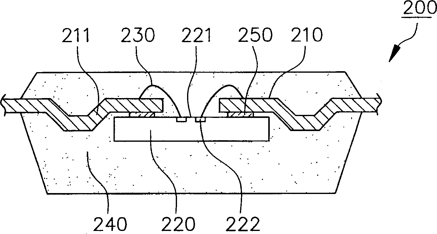
The invention relates to a semi-conductor encapsulation structure, which improves the wafer displacement when moulding die, and a lead wire bracket used. The semi-conductor encapsulation structure mainly comprises a plurality of pins containing a lead wire bracket, a wafer and a die closure colloid. The pins are divided, from the outer edge of the die closure colloid to the inter edge, into a plurality of first horizontal pins, a plurality of inclined pins and a plurality of second horizontal pins. A first bending line is formed at the connection part between the inclined pins and the corresponding first horizontal pins, and is close to or at one edge of the die closure colloid. A second bending line is formed at the connection part between the inclined pins and the corresponding second horizontal pins, and is close to one side of the wafer to make the inclined pins possess enough length for scattering the vertical model flow pressure difference and improving the problem of the vertical position displacement of the wafer.

Description

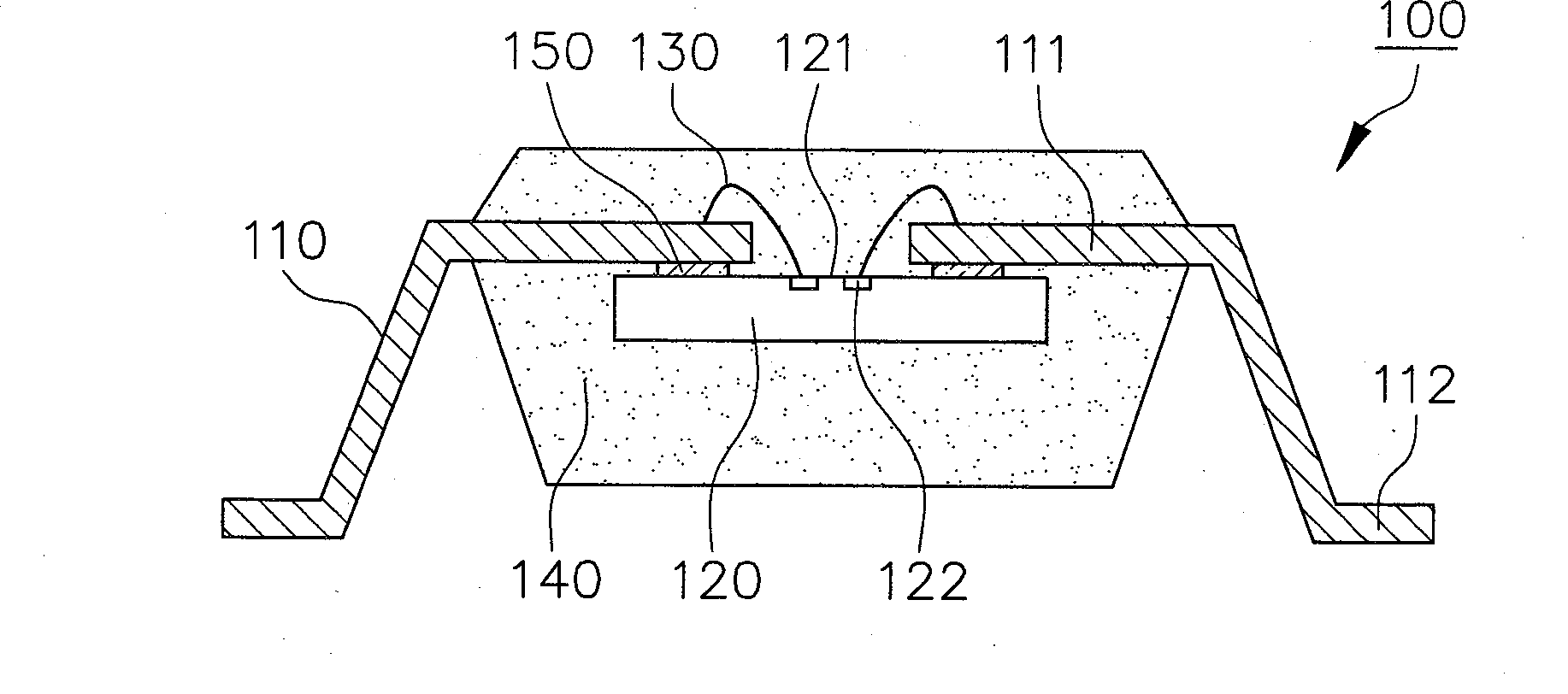
technical field [0001] The invention relates to a semiconductor package structure, in particular to a semiconductor package structure with inclined lead portions formed between different horizontal lead portions to improve chip displacement during compression molding and a lead frame used therefor. Background technique [0002] In the conventional semiconductor package structure, the leads of the lead frame are usually divided into horizontal inner leads and outer leads. During compression molding, a mold flow pressure is generated, which acts on the horizontal inner pins and the chip, causing the chip to produce a vertical position shift. [0003] see figure 1 Shown is a schematic cross-sectional view of a conventional semiconductor package structure. A conventional semiconductor package structure 100 includes a plurality of pins 110 of a LEAD-ON-CHIP (LOC) lead frame, a chip 120, a plurality of electrical connection elements 130 and a molding compound 140. The pins 110...

Claims


Application Information

Patent Timeline
Patent Type & Authority Patents(China)
IPC IPC(8): H01L23/495
CPCH01L2224/48091H01L2224/4826H01L2224/73215H01L2224/73265
Inventor 潘玉堂周世文吴政庭
Owner CHIPMOS TECH INC
Learn More