
An automatic operation system of inner leading bonding device of semiconductor device

A technology of welding equipment and operating system, which is applied in the improvement field of microelectronic packaging equipment from manual to automatic, which can solve the problems of high human resources and labor intensity, unstable work efficiency, inconsistent product performance, etc., and reduce labor intensity , Improve the scope of application and use value, and ensure the effect of consistency and stability

Inactive Publication Date: 2008-07-09
CHANGCHUN INST OF OPTICS FINE MECHANICS & PHYSICS CHINESE ACAD OF SCI +1
View PDF0 Cites 12 Cited by
  • Summary
  • Abstract
  • Description
  • Claims
  • Application Information

AI Technical Summary

Problems solved by technology

At present, most of the inner lead welding equipment introduced in my country are gold wire ball welding machines. The cost of gold wire is very high. In order to reduce production costs, ultrasonic aluminum wire pressure welding machines have been developed in China, but they can only be operated manually, and the welding depends on the alignment of human eyes. , for the microelectronics industry, manual operation consumes a lot of human resources and labor intensity, and the inconsistency of manual operation also causes instability in product performance and low work efficiency

Method used


Image

  • An automatic operation system of inner leading bonding device of semiconductor device
  • An automatic operation system of inner leading bonding device of semiconductor device
  • An automatic operation system of inner leading bonding device of semiconductor device

Examples


Embodiment Construction

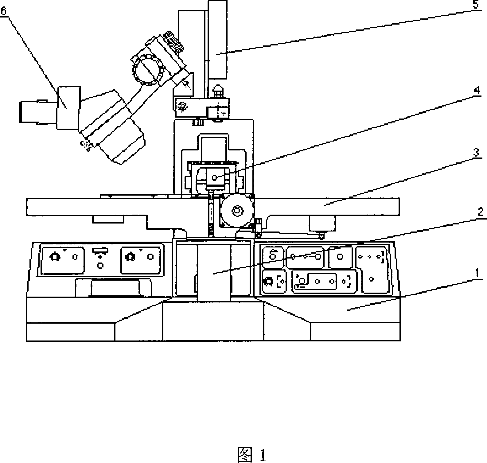
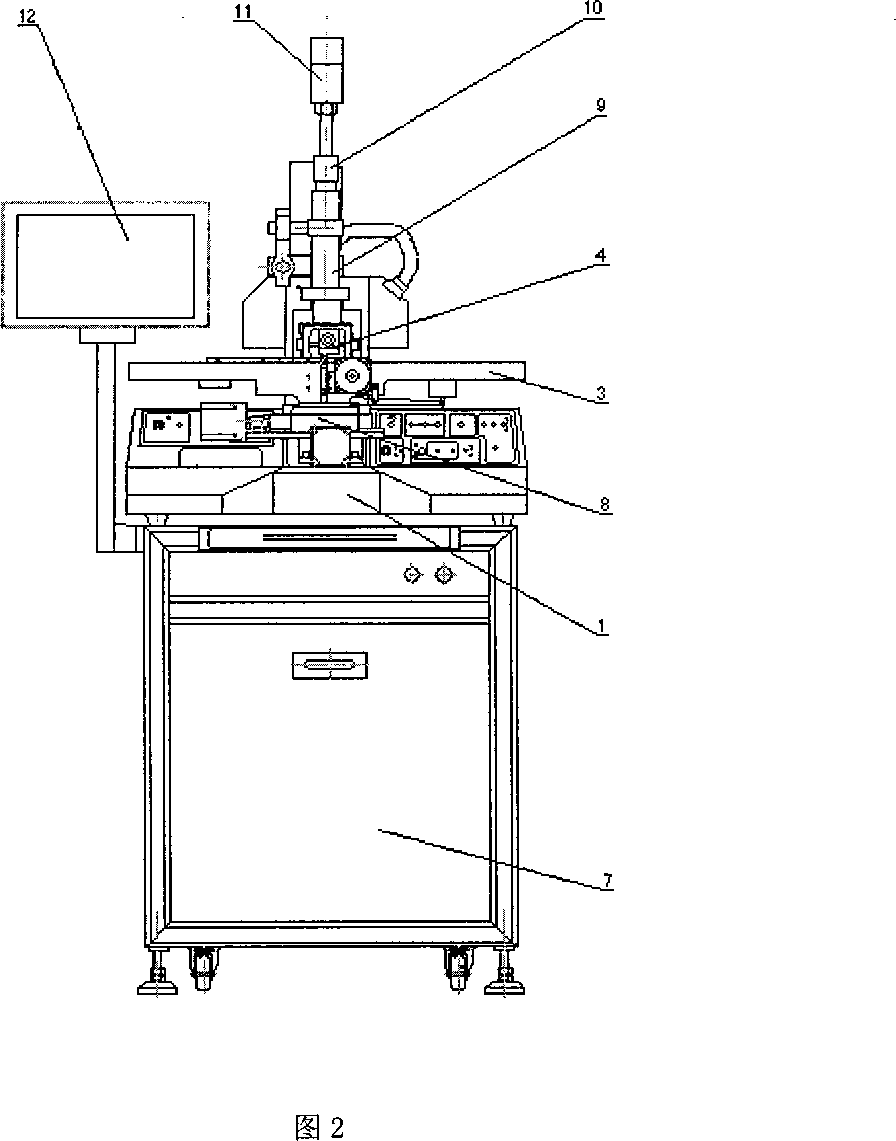
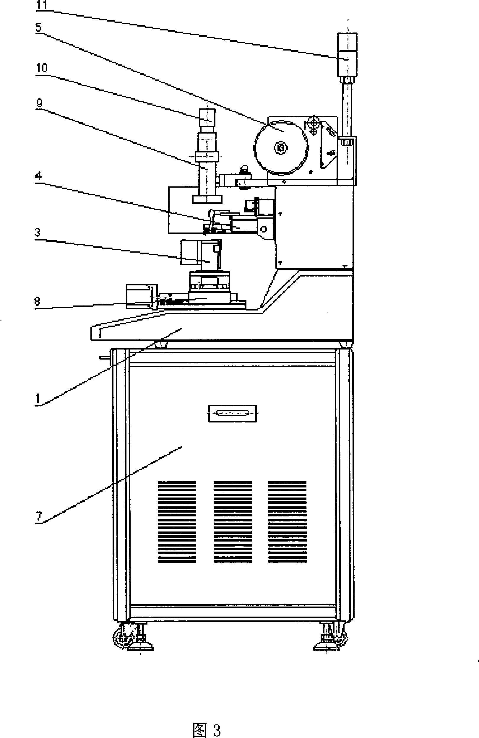
[0017] The present invention will be described in detail below in conjunction with the accompanying drawings. Taking the manual ultrasonic aluminum wire pressure welding machine as an example, the original manual ultrasonic aluminum wire pressure welding machine solder joint alignment is to use a microscope to observe with human eyes, and the operator keeps staring at the welder. In this area, the damage to human eyes is very large. Because of misoperation when people are tired or inattentive, resulting in a high product rejection rate and a decline in product quality. The improved model removes the microscope 6 on the original welding machine, and replaces it with the lens 9, CCD 10, and the image acquisition card in the main box 7 to jointly realize the image acquisition of the chip, and automatically identify the position of the chip through software processing. Manpower is liberated and product quality is improved.

[0018] The displacement of the fixture on the original m...


PUM


Abstract

The invention relates to an automatic operating system of welding equipment of lead wires in a semiconductor device, which pertains to the improvement of microelectronic encapsulation equipment from manual to automatic operation. The invention removes a clamp base, a microscope and increases an X-Y two-dimensional electric control platform, a lens, a CCD, a main case, a warning light and a display on the basis of an original manual machine table, the automatic displacement of a clamp or a welding head is realized by the X-Y two-dimensional electric control platform and a step motion control card in the main case, the CCD, the lens and an image collection card in the main case are arranged above the welding head to realize the automatic identification of the chip, and the automatic control of the welding is realized by a main control computer in the main case, so as to become the equipment for automatic welding. The invention can improve the product quality and the production efficiency, ensure the consistency and stability of the welding wires, save the human resources and reduce the labor intensity. The invention can greatly improve the application range and using value of a welding wire machine. The invention is high-tech microelectronic production equipment which integrates precision machinery, automatic control, image identification, computer application, ultrasonic welding and other various fields.

Description

technical field [0001] The invention relates to an automatic operating system for welding equipment for inner leads of semiconductor devices, which belongs to the improvement of microelectronic packaging equipment from manual to automatic. It transforms the manual operation of the wire welding equipment in the semiconductor device into an automatic welding equipment. Background technique [0002] In my country, microelectronic packaging equipment is currently imported from the United States, South Korea, and Japan. It is an important task to promote my country's modern high-tech to develop my country's microelectronic packaging equipment as soon as possible. At present, most of the inner lead welding equipment introduced in my country are gold wire ball welding machines, and the cost of gold wire is very high. In order to reduce production costs, ultrasonic aluminum wire pressure welding machines have been developed in China, but they can only be operated manually, and the w...

Claims


Application Information

Patent Timeline
IPC IPC(8): H01L21/607B23K20/10B23K101/40
CPCH01L2924/0002
Inventor 高跃红宋志郑福志
Owner CHANGCHUN INST OF OPTICS FINE MECHANICS & PHYSICS CHINESE ACAD OF SCI
Learn More