
Scanning electron microscope in situ electric measuring apparatus

An electron microscope and measuring device technology, applied in measuring devices, measuring electricity, measuring electrical variables, etc., can solve the problems of the length of electrode nanowires and the inability to change the position of electrodes, poor in-situ real-time observation ability, and small structure of nanomaterials. To achieve the effect of selectivity, reliable performance and convenient preparation

Inactive Publication Date: 2008-07-09
BEIJING UNIV OF TECH
View PDF0 Cites 9 Cited by
  • Summary
  • Abstract
  • Description
  • Claims
  • Application Information

AI Technical Summary

Problems solved by technology

At present, the main methods for in-situ testing of the electrical properties of nanoscale micro-units are mainly 1. Based on the focused ion beam FIB (focus iron beam) technology, electrodes are deposited at both ends of the object to be tested for measurement, but once the circuit is built, the gap between the electrodes Neither the length of the nanowire nor the position of the electrodes can be changed
2. Use the atomic force microscope to directly use the needle tip as an electrode to contact the unit under test and apply voltage to measure. The advantage is that the measurement is accurate, but the disadvantage is that the in-situ real-time observation ability is poor, and the sample in the plane of the sample stage cannot be measured
[0003] The scanning electron microscope is a powerful tool for studying the structure and properties of nanomaterials due to its convenient operation and large sample chamber space. However, due to the small structure of nanomaterials, it is difficult to manipulate and not use FIB for processing. How to directly test the unit in the scanning electron microscope Conducting electrical measurements and revealing the electrical properties and electric field effects of the unit under test in situ is a difficult problem in current nanomechanics research

Method used


Image

  • Scanning electron microscope in situ electric measuring apparatus

Examples


Embodiment Construction

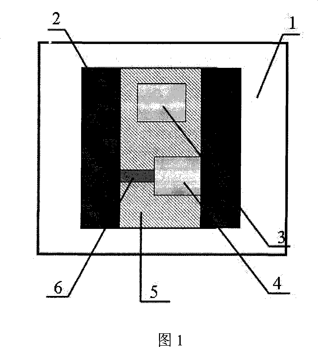
[0017] Below in conjunction with Fig. 1, the present invention will be further described:

[0018] Using a scanning electron microscope, it is possible to measure the electrical properties of micro-components under the condition of an applied electric field, observe the structural changes of the micro-components under the condition of an applied electric field in real time, directly correspond the electrical properties of the micro-units to the microstructure, and reveal nanowires or nanowires at the atomic level. Electrical properties and conduction mechanisms of microdevices.

[0019] This embodiment is an electrical measurement platform for micro devices. The electrical measurement platform includes a supporting part and a circuit part. The supporting portion is an insulating substrate 1 . The circuit part is two opposite metal electrodes 2 and the components to be measured 3, 4 and the phase change material film 5 between them. The metal electrode is bonded to the insul...


PUM


Abstract

The invention relates to a device for electrical measurement of miniature elements in scanning electron microscope, in particular to an in-situ electrical measurement device of scanning an electron microscope, which belongs to the field of in-situ performance measurement of nanomaterials. The device comprises a support portion and a circuit portion, wherein the support portion is an insulation substrate (1); the circuit portion includes two electrodes (2) fixed on the insulation substrate (1), an element (4) to be measured and a phase-change material amorphous thin film (5); the phase-change material amorphous thin film (5) is uniformly distributed between the two metal electrodes; and the element to be measured is positioned in the phase-change material amorphous thin film or concentrated on the metal electrodes. The connection line of the invention has erasable characteristics, and the phase-change material can be non-crystallized completely by applying higher voltage on both ends of the electrodes or directly irradiating a grid with a certain laser pulse to eliminate current path that has been formed, thus achieving selectivity and erasing ability of measurement circuits.

Description

technical field [0001] The invention relates to a device for electrical measurement of a micro-element to be measured in a scanning electron microscope, in particular to a scanning electron microscope in-situ electrical measurement device, which belongs to the field of in-situ measurement of nanometer material properties. Background technique [0002] With the development of nanotechnology and the development of nanodevices, the electrical properties and electric field effects of nanowires or other microunits under the action of external fields, especially electric fields, will definitely affect the reliability of devices, so the study of nanowires or microunits under the action of electric fields The electrical response and service behavior under the environment and the accumulation of electrical performance data are the basic standards for the current design and development of nano-devices. At present, the main methods for in-situ testing of the electrical properties of na...

Claims


Application Information

Patent Timeline
Patent Type & Authority Applications(China)
IPC IPC(8): G01R31/00
Inventor 张泽王珂刘攀韩晓东
Owner BEIJING UNIV OF TECH
Learn More