
Wafer-grade chip packaging process and chip packaging structure

A chip packaging structure, wafer-level chip technology, applied in semiconductor/solid-state device manufacturing, electrical components, electrical solid-state devices, etc., can solve the problems affecting the path of external incident light signals, optical signal distortion, residual air bubbles, etc. To achieve the effect of protecting the photosensitive area

Active Publication Date: 2008-07-02
ADVANCED SEMICON ENG INC
View PDF0 Cites 15 Cited by
  • Summary
  • Abstract
  • Description
  • Claims
  • Application Information

AI Technical Summary

Problems solved by technology

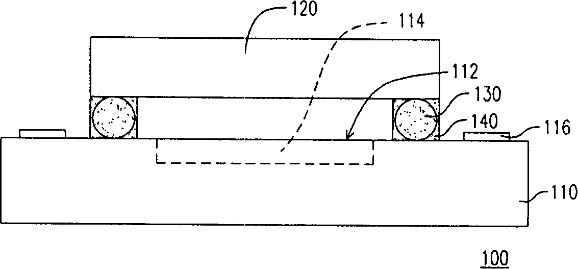
[0005] However, the adhesive layer 140 of the conventional chip packaging structure 100 usually has voids or bubbles remaining therein.
In addition, since there is still a gap between the transparent cover plate 120 and the chip 110, if particles remain therein during the packaging process, it will contaminate or scratch the photosensitive area 114, thereby affecting the path of external incident light signals, resulting in The optical signal received by the photosensitive area 114 is distorted

Method used


Image

  • Wafer-grade chip packaging process and chip packaging structure
  • Wafer-grade chip packaging process and chip packaging structure
  • Wafer-grade chip packaging process and chip packaging structure

Examples


Embodiment Construction

[0022] Figure 2A to Figure 2F A schematic side view of a wafer-level chip packaging process according to an embodiment of the present invention is shown. The wafer-level chip packaging process of this embodiment includes the following steps. First, please refer to Figure 2A , providing a wafer W. The wafer W includes a plurality of chip units C, and the wafer W has an active surface 212 and an opposite back surface 214 . Each chip unit C has a plurality of pads 216 on the active surface 212, and the material of the pads 216 includes aluminum.

[0023] Next, please refer to Figure 2B , forming a plurality of through holes 218 under the pads 216 . In this embodiment, the method of forming the through holes 218 includes etching, for example, using a laser to etch from the backside 214 of the wafer W to the pads 216 .

[0024] Next, please refer to Figure 2C The conductive material M is filled in these through holes 218, and the conductive material M in each through hol...


PUM


Abstract

A process for encapsulating a wafer level chip comprises the following steps that: first, a wafer is provided and a plurality of chip units are contained in the wafer, and the wafer has an active surface and a back facing to the active surface; each chip unit is provided with a plurality of connective cushions on the active surface and then a plurality of through holes are formed below the connective cushions, and then the conductive materials are stuffed in the through holes and are electrically connected with the connective cushions; moreover, the conductive materials are exposed and convex out from the back of the wafer. Then a transparent adhesive layer is formed on the active surface and then a transparent cover plate is configured on the transparent adhesive layer so as to bond the transparent cover palte with the wafer through the transparent adhesive layer. Then a step of monomerisation is carried out so as to separate the chip units from the transparent cover plate corresponding to the chip units, thereby forming a plurality of independent chip package structure.

Description

technical field [0001] The present invention relates to a packaging process and packaging structure, and in particular to a wafer-level chip packaging process and chip packaging structure. Background technique [0002] In the semiconductor industry, the production of integrated circuits (IC) is mainly divided into three stages: wafer manufacturing, IC process, and IC package. Among them, the chip (chip) is completed through the steps of wafer fabrication, circuit design, mask (mask) fabrication, and wafer sawing, and each chip formed by wafer dicing is After the contacts on the chip are electrically connected to external signals, the chip can be covered with a molding compound. The purpose of its packaging is to prevent the chip from being affected by moisture, heat, and noise, and to provide a medium for electrical connection between the chip and the external circuit, thus completing the packaging step of the integrated circuit. [0003] However, since the traditional int...

Claims


Application Information

Patent Timeline
IPC IPC(8): H01L21/50H01L21/56H01L21/60H01L23/10H01L23/31H01L23/482
CPCH01L24/94H01L2924/14H01L2924/181
Inventor 陈建宇
Owner ADVANCED SEMICON ENG INC
Learn More