
Semiconductor technology

A semiconductor and process technology, applied in the field of metal material hard mask technology, can solve the problems of substrate particle precipitation and process defects

Active Publication Date: 2008-07-02
UNITED MICROELECTRONICS CORP
View PDF0 Cites 7 Cited by
  • Summary
  • Abstract
  • Description
  • Claims
  • Application Information

AI Technical Summary

Problems solved by technology

[0006] However, when using halothane gas plasma, such as CH 2 f 2 or CHF 3 When plasma is used to remove the etching process of the cap layer 14, due to the existence of fluorine radicals, titanium-fluorine compound particles are often formed with the titanium component of the hard mask and distributed on the surface of the substrate, causing process defects, which is not acceptable. desire, but a problem to be solved
[0007] Therefore, there is still a need for a better semiconductor manufacturing method to solve the above-mentioned problem of particle precipitation on the substrate in the presence of fluorine-containing radicals using a titanium-containing hard mask

Method used


Image

  • Semiconductor technology
  • Semiconductor technology
  • Semiconductor technology

Examples


Embodiment Construction

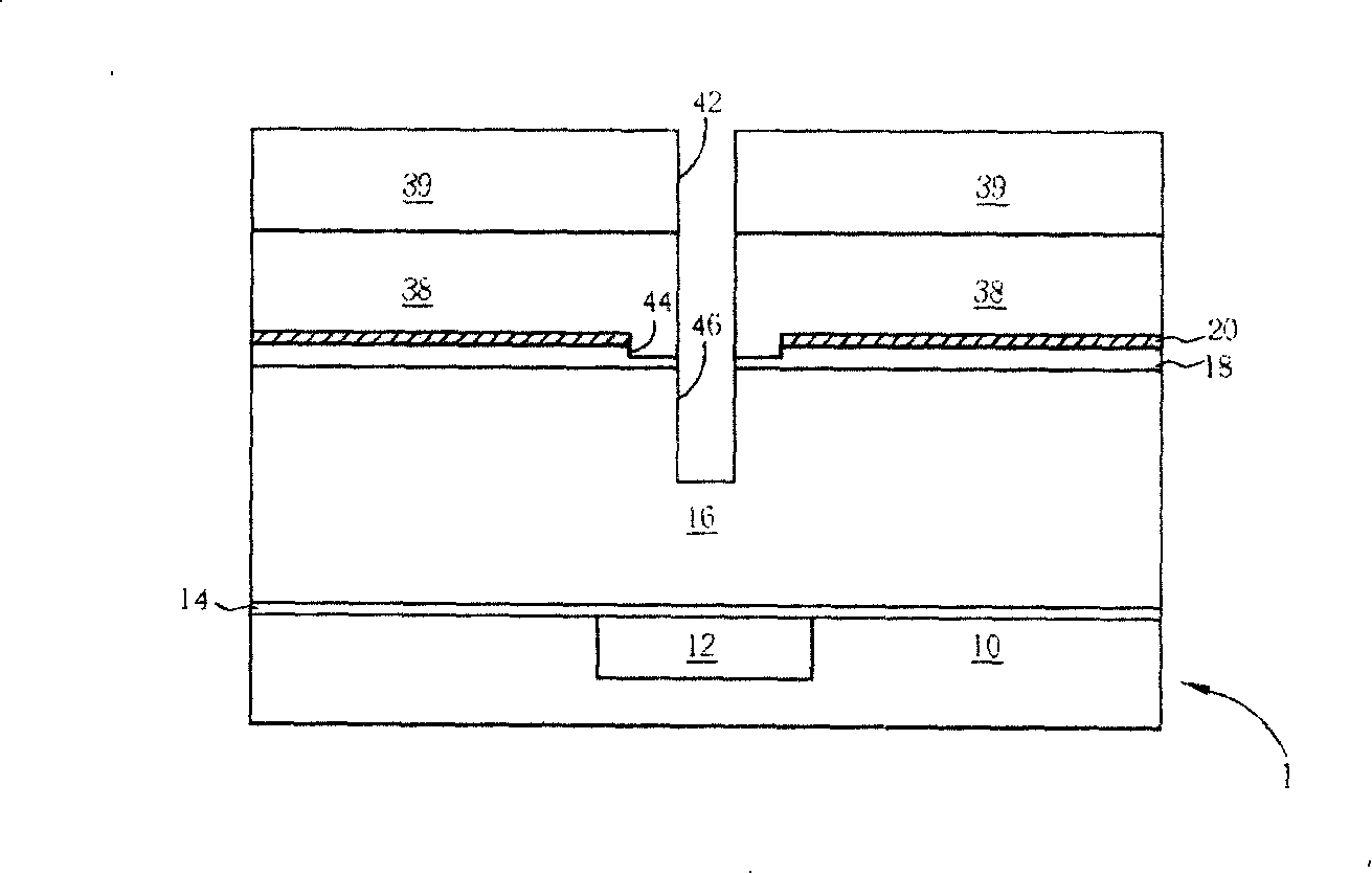
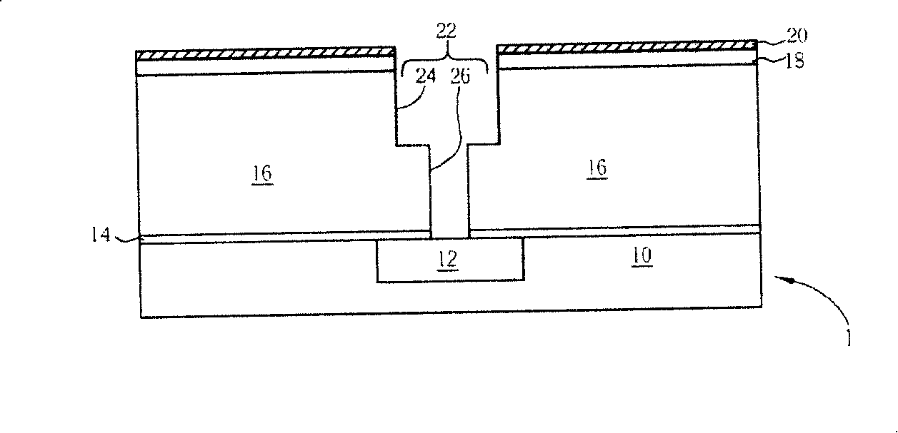
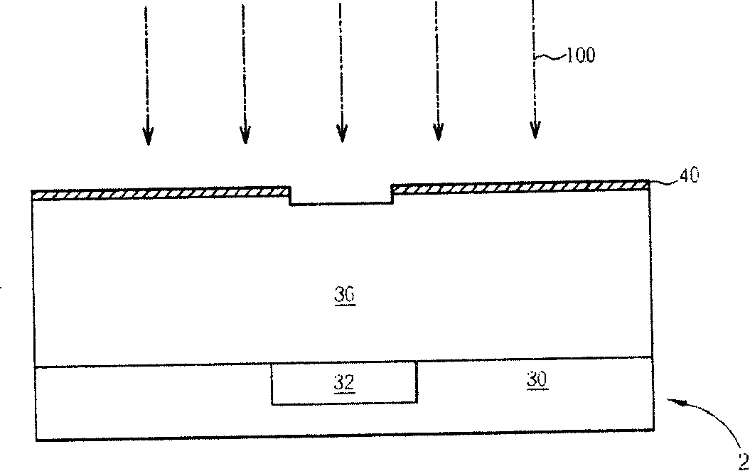
[0030] see image 3 and Figure 4 , which shows a schematic cross-sectional view of a specific embodiment of the semiconductor process according to the present invention, which uses a damascene process for illustration. The same symbols are still used to represent the same or similar elements or regions. It should be emphasized that the present invention is not limited to those disclosed in the figures, any hard mask, especially a hard mask containing titanium (Ti) components, such as titanium metal or titanium nitride, and the use of fluorine-containing radical gas Etching processes, such as, but not limited to, several damascene or dual damascene processes, can use the method of the present invention. The dual damascene process can be, for example, trench-first, via-first, partial via-first and other damascene processes.

[0031] Such as image 3 As shown, the substrate 2 may be a semiconductor substrate including an underlying or dielectric layer 30 . Formed in the die...


PUM


Abstract

The invention discloses a semiconductor process, which comprises the following steps: a plasma containing the fluorine free radicals is used for etching a characteristic pattern on a rigid mask and in a layer below the rigid mask, and a gas which can react with the fluorine free radicals is used for carrying out the treatment to ensure that the residual fluorine free radicals react with the gas so as to form the fluorine-contained compounds for the purpose of removal, thereby preventing the fluorine free radicals from reacting with the titanium compositions with forming the particles deposited on a substrate, which results in the process defect.

Description

technical field [0001] The invention relates to a semiconductor process, in particular to a process using a metal material hard mask in the semiconductor process. Background technique [0002] With the progress of the semiconductor industry, in order to comply with the development and design of such high-density integrated circuits, the dimensions of various components are reduced to sub-micron. There are many technologies that use masks in the semiconductor process. [0003] For example, with the current trend of continuously reducing the size of integrated circuits, integrated circuit technology has been developed towards the direction of multiple metal interconnects. In order to solve the difficulty of fabricating metal interconnections in multi-layers, the damascene process has been extensively researched and developed. A hard mask is used in the damascene process. In addition, because copper (Cu) has a lower resistivity and excellent electron migration (electromigrat...

Claims


Application Information

Patent Timeline
IPC IPC(8): H01L21/00H01L21/311H01L21/768
Inventor 赖育聪黄俊仁姚志成廖俊雄
Owner UNITED MICROELECTRONICS CORP
Learn More