Bonding sheet for capacitor and method for manufacturing capacitor built-in printing wiring board
A technology for printed wiring boards and manufacturing methods, applied in the direction of multilayer circuit manufacturing, semiconductor/solid-state device manufacturing, electric solid-state devices, etc., to achieve cheap and stable manufacturing, and the effect of stabilizing electrostatic capacitance
- Summary
- Abstract
- Description
- Claims
- Application Information
AI Technical Summary
Problems solved by technology
Method used
Image
Examples
Embodiment 1
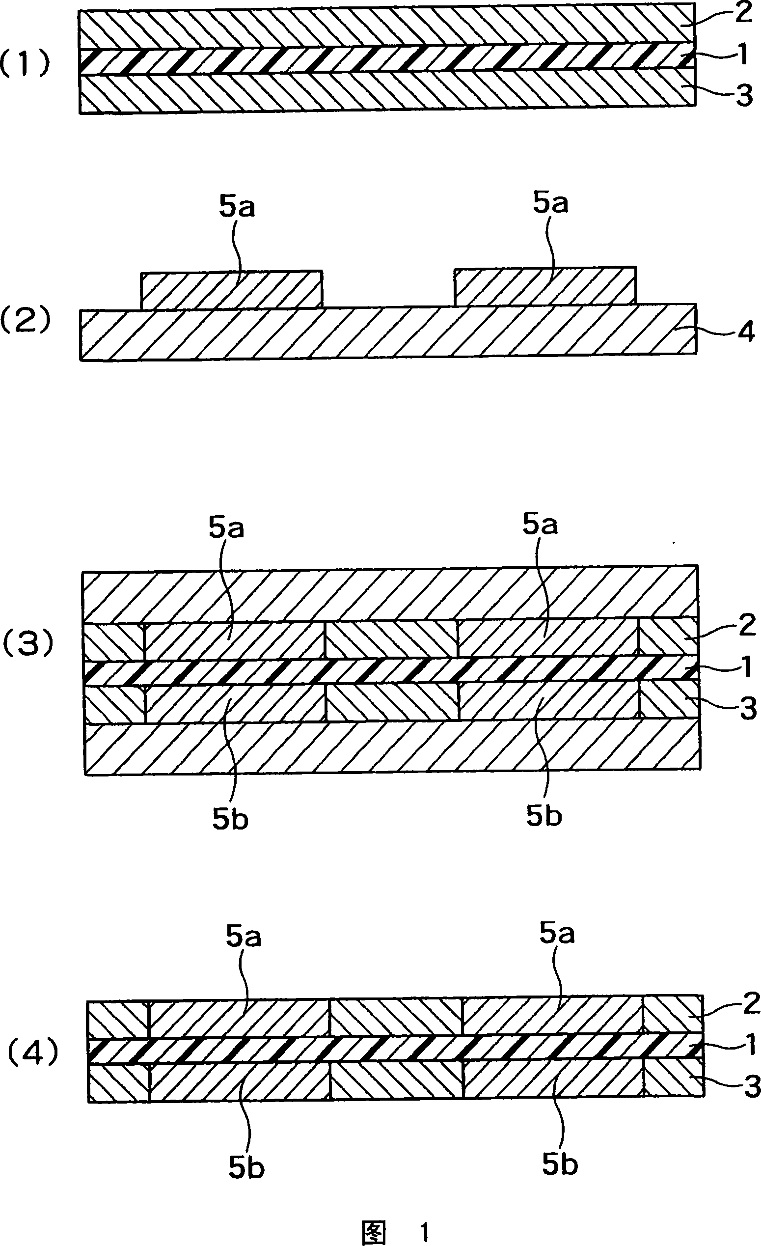
[0052] FIG. 1 is a cross-sectional process diagram showing a method of manufacturing an adhesive sheet for capacitors in Example 1 of the present invention. First, as shown in FIG. 1(1), a base material having high fluidity adhesive resin layers 2 and 3 on both surfaces of a high dielectric constant and low fluidity dielectric layer 1 is prepared. Here, the dielectric layer 1 is a film-shaped molded product having a dielectric constant of about 2000 and containing about 60 to 85% by weight of barium titanate, and about 15 to 40% by weight of a solvent portion and an epoxy resin.
[0053] The relative dielectric constant of this film-like molded article is about 20-60. Regarding the thickness, it is preferable to be as thin as possible within the range that does not cause film defects such as pinholes, and a thickness of 5 to 30 μm is also suitable because of its flexibility. However, if a single body is used, it is brittle and prone to tearing, so the flow of various processe...
Embodiment 2
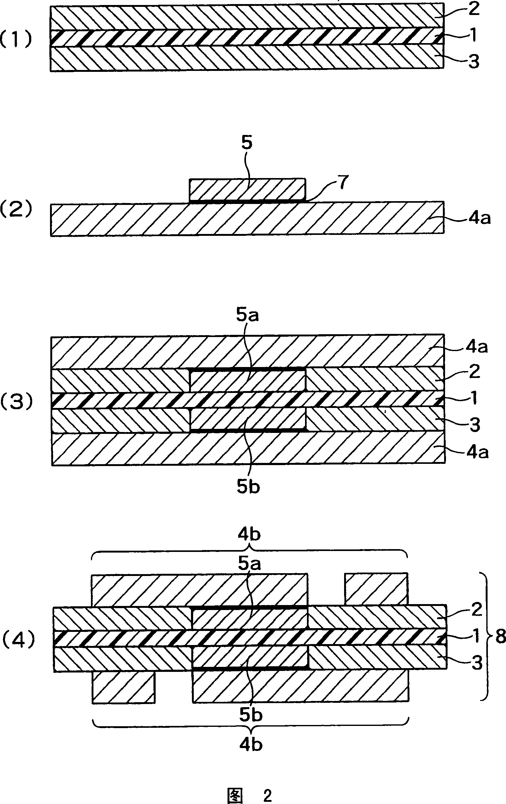
[0076] 2 is a cross-sectional process view showing a method of manufacturing a capacitor in Example 2 of the present invention. First, as shown in FIG. 2(1), prepare adhesive resin layers 2 and 3 with high fluidity on both sides of a dielectric layer 1 with high dielectric constant and low fluidity as shown in FIG. 1(1). base material.
[0077] Next, as shown in FIG. 2(2), prepare a metal base material having a three-layer structure of copper foil 4a (for example, a thickness of 18 μm) / nickel foil 7 (for example, a thickness of 2 μm) / copper foil 5 (for example, a thickness of 18 μm). , the electrode portion 5a is formed by selective etching in the photoprocessing method.
[0078] In addition, although not shown in figure, the electrode part 5b which opposes is formed in the copper foil 4a. The exposed nickel foil other than the electrode portion was removed by selective etching, and a roughening treatment for improving the adhesion strength between the copper foil and the ad...
Embodiment 3
[0086] 3 is a cross-sectional process view showing a method of manufacturing a capacitor in Example 3 of the present invention. First, as shown in FIG. 3(1), prepare the substrate shown in FIG. 1(1) with high fluidity adhesive resin layers 2, 3 on both sides of the dielectric layer 1 with high dielectric constant and low fluidity. Material.
[0087] Next, as shown in FIG. 3(2), a so-called double-sided copper-clad laminate having copper foils 10 and 11 on both sides of a polyimide film 9 having a thickness of 25 μm is prepared, and is processed by selective etching in a photoprocessing method. The electrode portion 10a is formed. In addition, although not shown in figure, the opposing electrode part 10b is formed on the polyimide film 9. As shown in FIG. And roughening process for improving the adhesive strength of copper foil and an adhesive material in a subsequent process is performed.
[0088] Next, as shown in FIG. 3 (3), the base material on which the electrodes 10a, ...
PUM
 Abstract
Description
Claims
Application Information
 - R&D
- Intellectual Property
- Life Sciences
- Materials
- Tech Scout
- Unparalleled Data Quality
- Higher Quality Content
- 60% Fewer Hallucinations
Browse by: Latest US Patents, China's latest patents, Technical Efficacy Thesaurus, Application Domain, Technology Topic, Popular Technical Reports.
© 2025 PatSnap. All rights reserved.Legal|Privacy policy|Modern Slavery Act Transparency Statement|Sitemap|About US| Contact US: help@patsnap.com


