
Mask plate territory for manufacturing connecting pore and its design method

A technology for manufacturing connections and design methods, which is applied in the field of mask template layout and design for manufacturing connection holes, can solve the problems of complex mask template manufacturing process and photolithography process, save time and economic cost, simple process, and improve consistency sexual effect

Inactive Publication Date: 2008-06-11
SEMICON MFG INT (SHANGHAI) CORP
View PDF1 Cites 10 Cited by
  • Summary
  • Abstract
  • Description
  • Claims
  • Application Information

AI Technical Summary

Problems solved by technology

[0005] Therefore, the object of the present invention is to provide a mask template layout and its design method for making connection holes, to solve the existing method of improving the consistency of isolated graphics and dense graphics depth of focus to make the mask template manufacturing process and photolithography process complicated question

Method used


Image

  • Mask plate territory for manufacturing connecting pore and its design method
  • Mask plate territory for manufacturing connecting pore and its design method
  • Mask plate territory for manufacturing connecting pore and its design method

Examples


Embodiment Construction

[0024] In order to make the above objects, features and advantages of the present invention more comprehensible, specific implementations of the present invention will be described in detail below in conjunction with the accompanying drawings.

[0025] With the development of semiconductor manufacturing technology to smaller technology nodes, the requirements for the resolution of lithography process are getting higher and higher. The resolution of lithography can be improved through high-resolution exposure light source, advanced mask correction technology (OPC) and immersion exposure technology. At present, the resolution of optical lithography has reached 45nm or even smaller. The improvement of lithography resolution has brought another problem, that is, the reduction of focus depth, which means that lithography can only achieve the required resolution within a small focal length range, and the process parameters on the production line A slight deviation will cause the lin...


PUM


Abstract

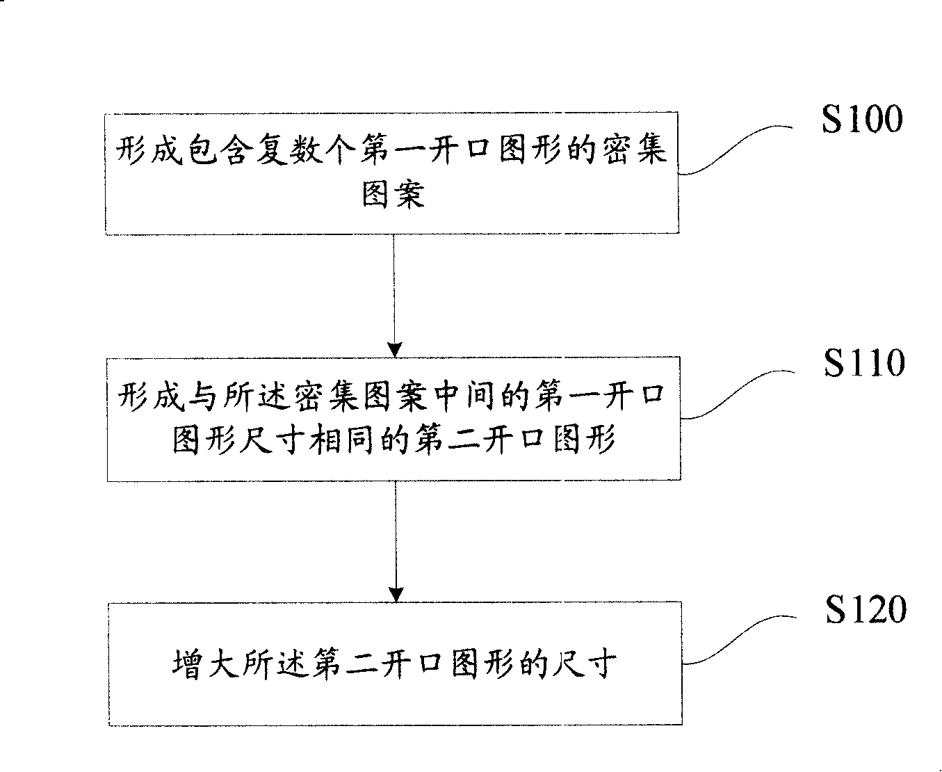
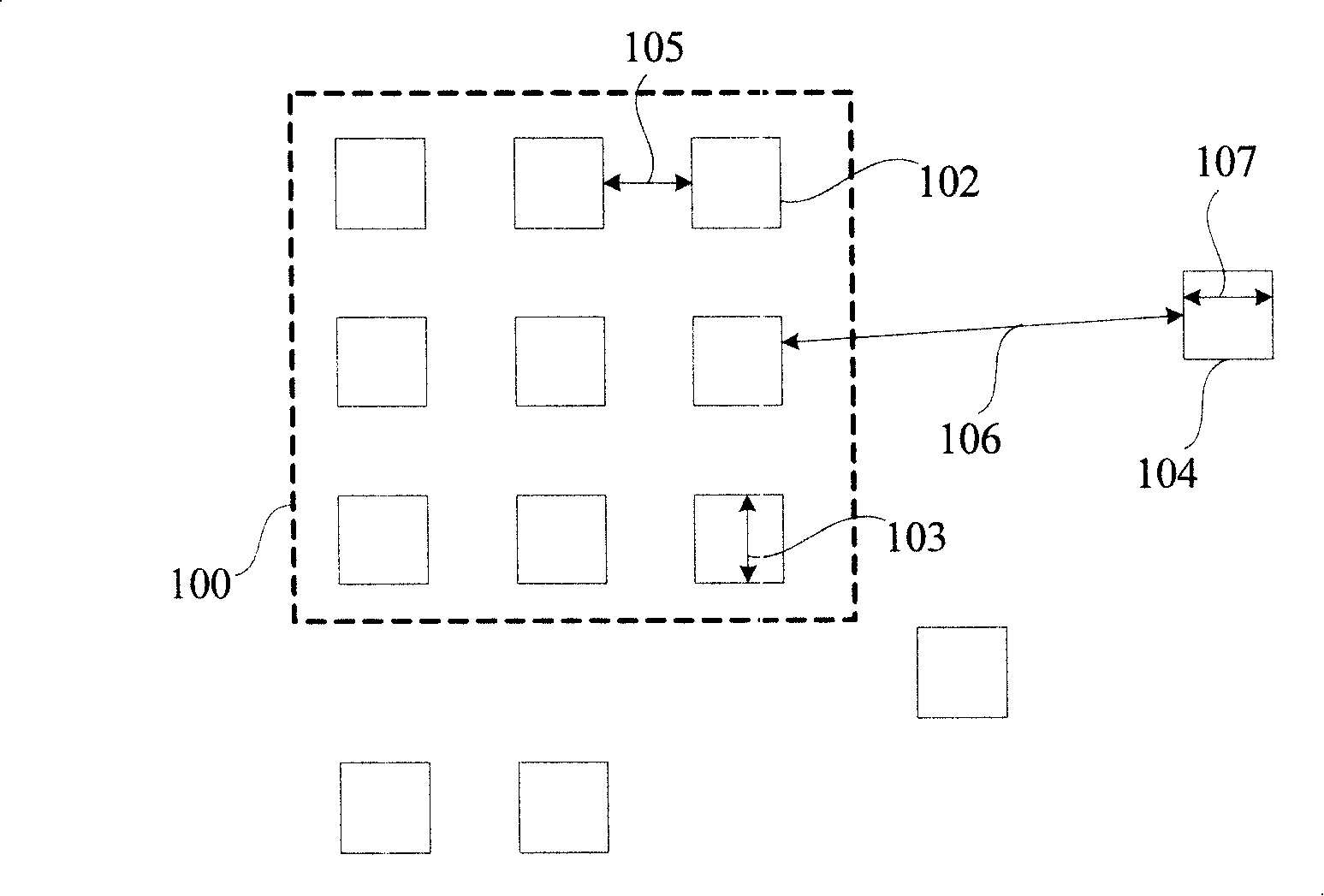
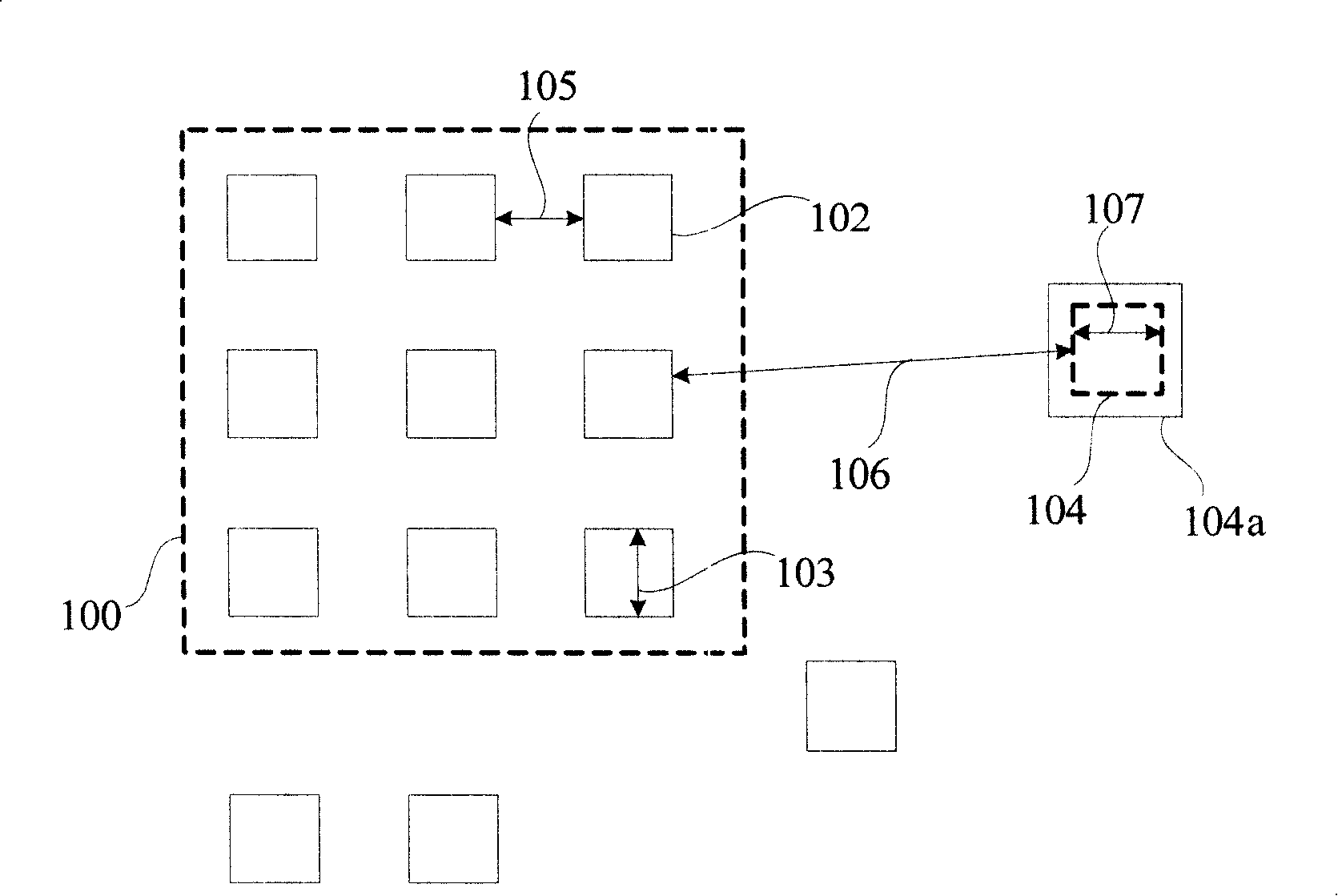
A design method of mask plate layout for manufacturing a connecting hole is provided, which comprises a dense pattern containing plural first opening figures is formed, an isolated second opening figure is formed, and the dimension of the second opening figure is larger than the dimension of the first opening hole figure of the dense pattern center; wherein, the first opening figure and the second opening figure are used for forming the connecting hole. The utility model can improve the consistency of the focus depth of the isolated figure and the dense figure, the manufacturing technics of the mask plate is simple and the cost is low.

Description

technical field [0001] The invention relates to the technical field of semiconductor manufacturing, in particular to a mask template layout for manufacturing connection holes in a photolithography process and a design method thereof. Background technique [0002] With the development of semiconductor technology to small line width and high integration, higher requirements are put forward for the photolithography process. The optical exposure wavelength has developed from 365nm to 248nm, and 193nm or even smaller. Immersion exposure technology based on high refractive index medium has also been developed. As the size of the device shrinks, the size of the pattern on the photolithography mask is getting smaller and smaller, and the pitch of the pattern is getting closer and closer. Optical interference and diffraction effects make the resolution of the pattern transferred to the wafer less than ideal. Traditional binary masks can no longer meet the needs of deep submicron lit...

Claims


Application Information

Patent Timeline
IPC IPC(8): G03F1/14G03F7/20H01L21/027G03F1/38
Inventor 林益世
Owner SEMICON MFG INT (SHANGHAI) CORP
Learn More