
Metal-insulator-metal capacitor and its manufacture process

A technology of metal capacitors and manufacturing methods, applied in semiconductor/solid-state device manufacturing, electrical solid-state devices, semiconductor devices, etc., can solve problems affecting the film deposition process, etc., and achieve the solution of reaction residues, excellent structure, and optimized manufacturing process Effect

Inactive Publication Date: 2008-06-04
SEMICON MFG INT (SHANGHAI) CORP
View PDF1 Cites 9 Cited by
  • Summary
  • Abstract
  • Description
  • Claims
  • Application Information

AI Technical Summary

Problems solved by technology

The Ta-based polymer 150 is attached to the side of the photoresist 105 that has not been removed. After the photoresist 105 is removed, the Ta-based polymer 150 remains on the side and top of the hard mask 104, forming a crown of residual polymer 160, such as Figure 2F As shown, it seriously affects the subsequent film deposition process

Method used


Image

  • Metal-insulator-metal capacitor and its manufacture process
  • Metal-insulator-metal capacitor and its manufacture process
  • Metal-insulator-metal capacitor and its manufacture process

Examples


Embodiment Construction

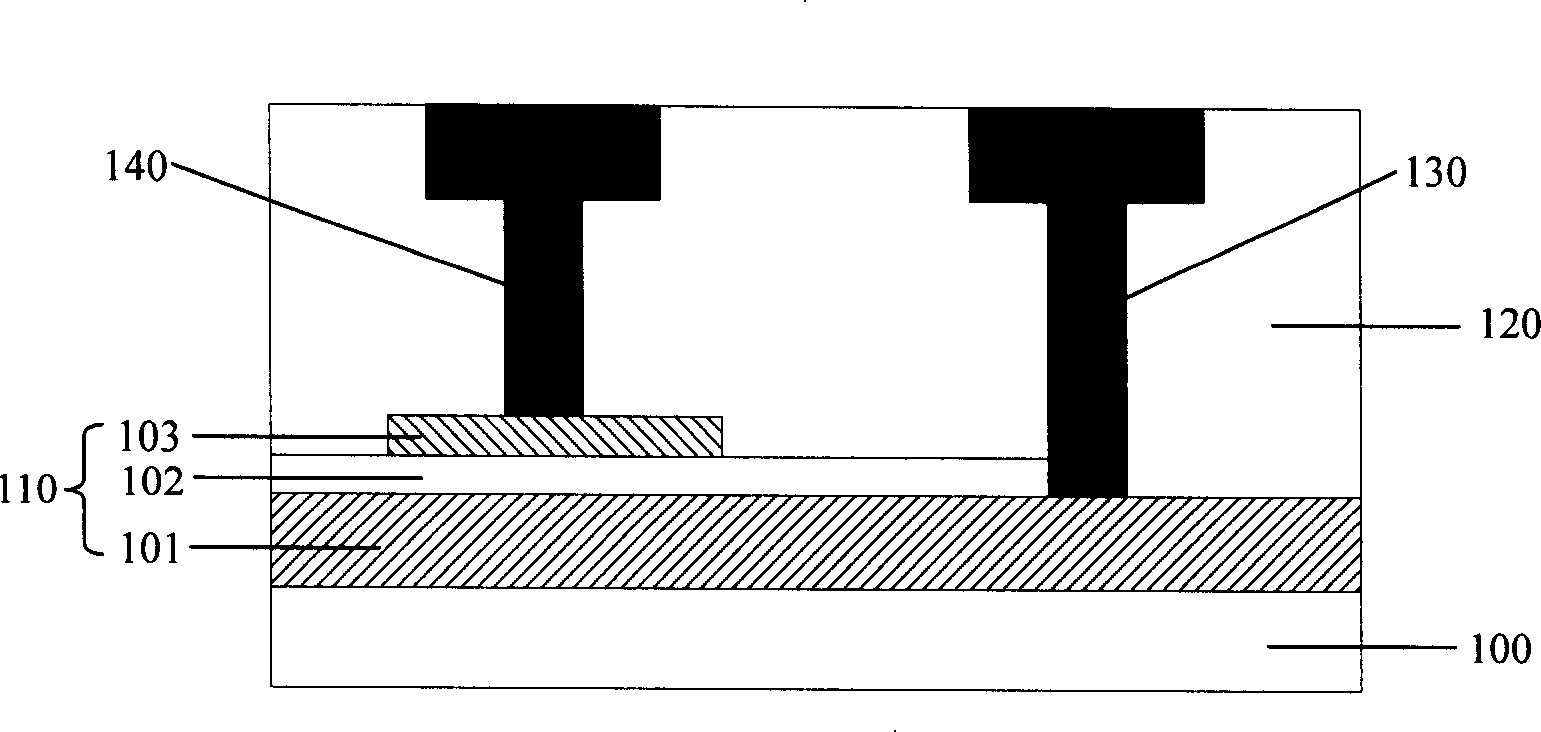
[0028] The invention relates to the technical field of semiconductor integrated circuit manufacturing, in particular to a method for forming a MIM capacitor in a semiconductor device and the MIM capacitor formed by the method. It should be noted here that the embodiments provided in this specification are used to illustrate various features of the present invention, and are only used for convenience of description by using specific compositions and structures, and are not intended to limit the present invention.

[0029] The manufacturing method of the metal-insulator-metal capacitor of the present invention adopts the method of single damascene to form the upper electrode of the MIM capacitor, that is, adopts the way of filling, and after forming the lower electrode metal layer and the dielectric layer, a layer of intermetallic layer is formed on the surface of the dielectric layer. dielectric layer (IMD), and use the photoresist as a mask to define the position of the upper e...


PUM


Abstract

The invention discloses a method for manufacturing a metal-insulator-metallic capacitor. The method includes the following steps: a first metallic layer is generated on an insulating layer; a first dielectric layer is generated on the first metallic layer; a second dielectric layer is generated on the first dielectric layer; a groove is generated in the second dielectric layer; a second metallic layer is generated in the groove; the second metallic layer and the second dielectric layer are processes by planarization till the surface of the second dielectric layer is exposed. The invention also accordingly discloses a metal-insulator-metallic capacitor, which includes a lower electrode plate generated on the insulating layer, the dielectric layer generated on the lower electrode plate, an upper electrode plate generated on the dielectric layer and the dielectric layer between metals generated before the upper electrode plate and on two sides of the upper electrode plate. The metal-insulator-metallic capacitor and the manufacturing method of the invention can avoid an appearance of defect with coronal etching.

Description

technical field [0001] The invention relates to the technical field of semiconductor manufacturing, in particular to a metal-insulator-metal (Metal-Insulator-Metal, MIM) capacitor and a manufacturing method thereof. Background technique [0002] Capacitors are widely used in semiconductor integrated circuits as charge storage, coupling, and filter devices. Generally, in order to improve the performance of high-speed digital circuits and radio frequency (RF) circuits, it is necessary to use large-capacity capacitors and adopt corresponding forming methods. As semiconductor technology enters the 90nm process node, the feature size of devices continues to shrink, and high-performance, high-density connections between components are not only interconnected in a single interconnect layer, but also interconnected between multiple layers. Therefore, a large number of connections between devices adopt a multilayer interconnection structure, in which multiple interconnection metal l...

Claims


Application Information

Patent Timeline
IPC IPC(8): H01L21/02H01L21/82H01L29/92H01L27/00
Inventor 沈满华胡友存
Owner SEMICON MFG INT (SHANGHAI) CORP
Learn More