
Chip resistor and its manufacturing method

A chip resistor and manufacturing method technology, applied in the direction of resistor manufacturing, resistors, thick film resistors, etc., can solve the problems such as impact applied by chip resistor 1, insufficient solder connection strength, damage, etc., to protect the appearance. Effect

Inactive Publication Date: 2008-05-28
KAO CORP
View PDF1 Cites 9 Cited by
  • Summary
  • Abstract
  • Description
  • Claims
  • Application Information

AI Technical Summary

Problems solved by technology

In addition, since the width dimension of the insulating substrate 2 is larger than the thickness dimension, when it is placed in the accommodation recess of the positioning jig (sample) in a horizontal posture, a part of the insulating substrate 2 protrudes greatly above the positioning jig. , so that there is a problem that shock is applied to the suction nozzle and the chip resistor 1 at the time of mounting and is easily damaged
[0008] In addition, although the miniaturization of chip resistors has been promoted in recent years, and for example, extremely small chip resistors with a length dimension of 1 mm and a thickness dimension of 0.5 mm are also becoming popular, it is difficult to manufacture such ultra-small chip resistors. Thick end-face electrodes are formed with high precision on a rectangular substrate, and the method of forming thin end-face electrodes by sputtering is generally used
However, when forming the end surface electrodes by sputtering, the side electrodes cannot be formed simultaneously in the divided grooves, so the solder connection strength is insufficient when the chip resistor is mounted on the circuit board in a lateral orientation.

Method used


Image

  • Chip resistor and its manufacturing method
  • Chip resistor and its manufacturing method
  • Chip resistor and its manufacturing method

Examples


Embodiment Construction

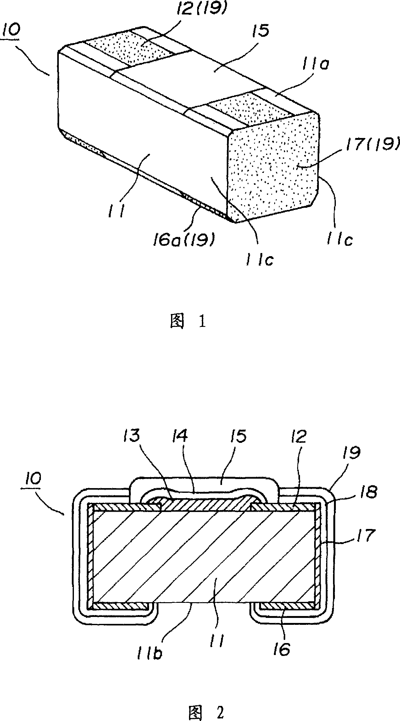
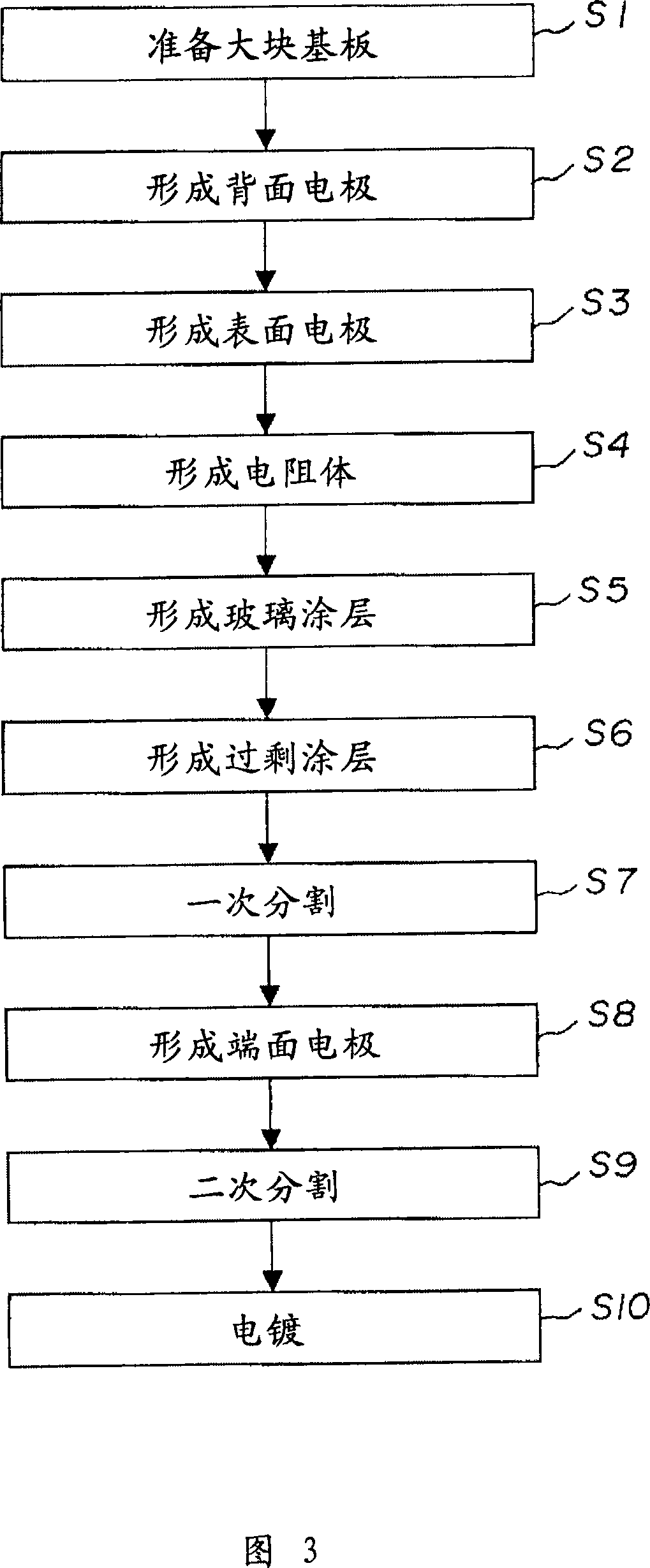
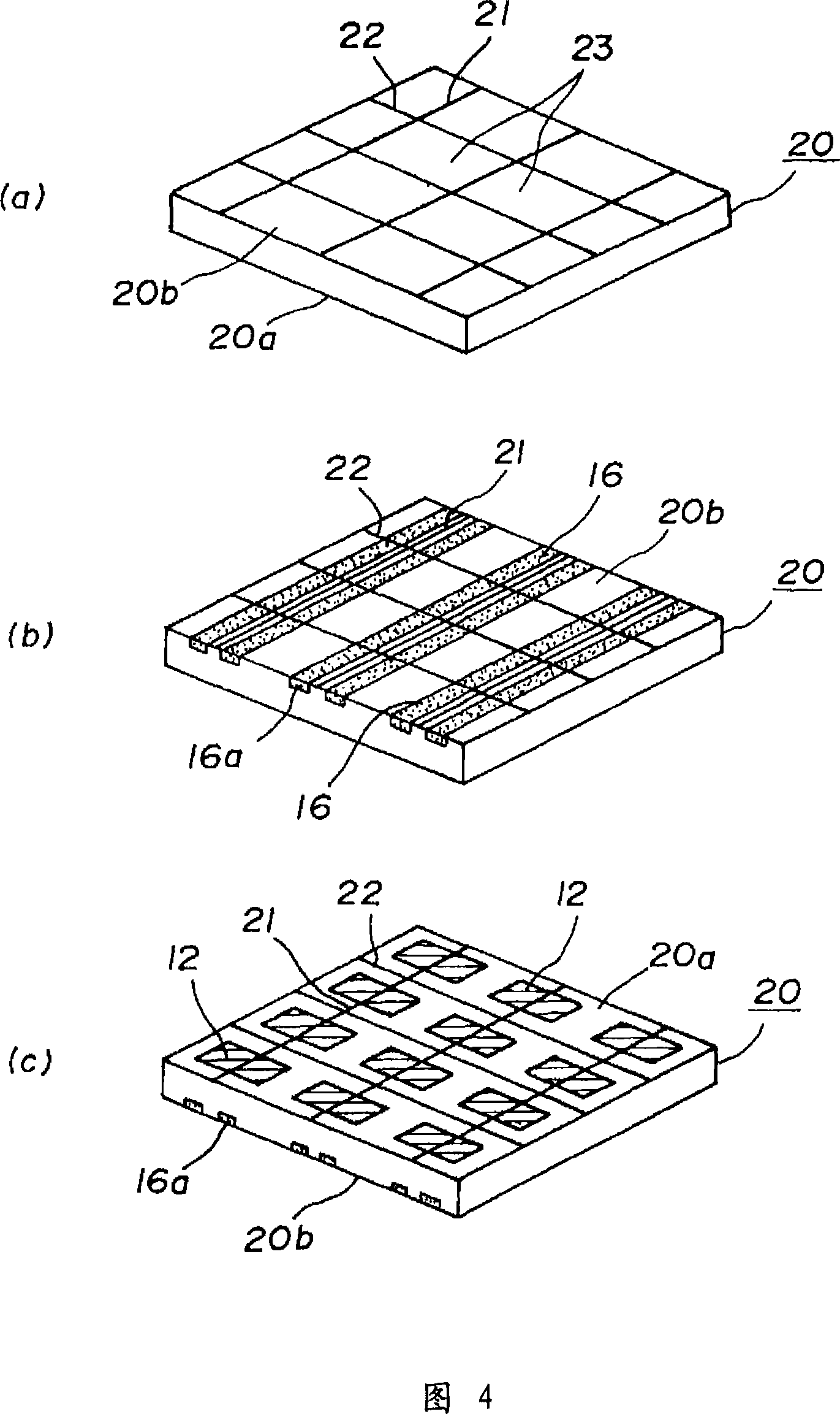
[0019] Embodiments of the present invention will be described with reference to the accompanying drawings. FIG. 1 is a perspective view of a chip resistor according to an example of this embodiment, FIG. 2 is a cross-sectional view schematically showing the chip resistor, and FIG. 3 is a diagram showing a manufacturing process of the chip resistor. 4 to 6 are explanatory diagrams showing the manufacturing method of the chip resistor in the order of steps, FIG. 7 is an explanatory diagram showing the state that the chip resistor is supplied to the sample in two different postures, and FIG. 8 is A side view showing a state in which the chip resistor is mounted on a solder pad in a lateral orientation.

[0020] The chip resistor 10 shown in these figures is a rectangular chip resistor corresponding to a multi-mounting method. A plurality of nozzles are sucked and mounted on the solder pads 33 of the circuit board 32 (see FIGS. 7 and 8 ). As shown in FIGS. 1 and 2 , the chip resi...


PUM

PropertyMeasurementUnit
sizeaaaaaaaaaa
sizeaaaaaaaaaa

Abstract

To provide a chip resistor so constituted that even if the chip resistor is mounted in a horizontal posture, the soldering strength is ensured, there is no apprehension that the chip resistor projects from the accommodation recess of a positioning tool in the mounting step, the promotion of miniaturization is not hindered, and the appearance of the chip resistor is favorable and its manufacturing method. When chip resistors (10) are produced, front electrodes (12) and resistor bodies (13) are fabricated in the front surface (20a) of a large board (20) and back electrodes (16) are fabricated on the back surface (20b) of the large board (20). When the back electrodes (16) are fabricated, the back electrodes (16) are extended on an inclining surface of V-grooves formed in the back surface (20b) as secondary split grooves (22) and the extending portions are used as side electrodes (16a). The large board (20) is cut along primary grooves (21) into rectangular pieces, edge electrodes (17) are formed on the cut surface by sputtering, and the rectangular boards (24) are cut along the secondary grooves (22) into chips. Each chip is plated, thus producing a chip resistor (10) having a shape of a generally rectangular solid and electrodes exposed on the sides.

Description

technical field [0001] The present invention relates to square chip resistors mass-mounted by multiple mounting methods and a manufacturing method thereof. Background technique [0002] Recently, the technique of mass-mounting chip components such as chip resistors by multiple mounting methods has become widespread. In this multi-mounting method, a positioning jig called a template is used, which is provided with a large number of accommodation recesses in accordance with the arrangement on the circuit board. After the chip components are removed, the chip components in the respective housing recesses are collectively mounted on the circuit board by a mounter having suction nozzles (nozzles), so that the mounting speed can be significantly improved. [0003] FIG. 9 is a perspective view showing a conventional square chip resistor corresponding to such a multiple mounting method (for example, refer to Patent Document 1). The chip resistor 1 shown in the same figure includes...

Claims


Application Information

Patent Timeline
Patent Type & Authority Applications(China)
IPC IPC(8): H01C7/00H01C17/00H01C17/16
CPCH01C1/148H01C1/01H01C1/144H01C7/003H01C17/006Y10T29/49082
Inventor 花冈敏博村濑真二
Owner KAO CORP
Learn More