Surface treatment, specification and assembling method for microelectronic element and its storage structure

A technology for microelectronic components and surface treatment, applied in electrical components, circuits, semiconductor/solid-state device manufacturing, etc., to solve the problems of chip corrosion, delamination, product debris, etc.

Inactive Publication Date: 2008-01-23
UNITED MICROELECTRONICS CORP
View PDF0 Cites 5 Cited by
  • Summary
  • Abstract
  • Description
  • Claims
  • Application Information

AI Technical Summary

Problems solved by technology

For example, after storing microelectronic components for a long time, it is found that the surface of the chip (chip) of the microelectronic components will have corrosion (corrosion), discoloration (discolor) or delamination (delaminating), which will lead to the deterioration of the final product. debris

Method used


Image

  • Surface treatment, specification and assembling method for microelectronic element and its storage structure
  • Surface treatment, specification and assembling method for microelectronic element and its storage structure
  • Surface treatment, specification and assembling method for microelectronic element and its storage structure

Examples


Embodiment Construction

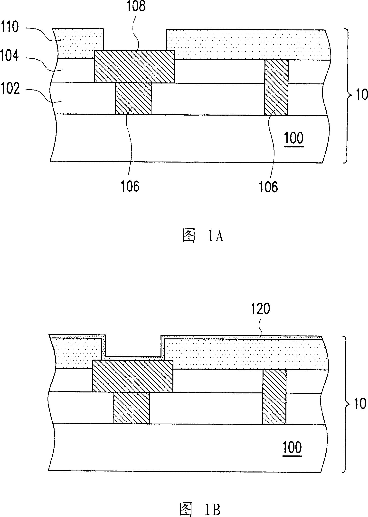
[0034] 1A to 1B are cross-sectional views of a surface treatment process of a microelectronic element according to a first embodiment of the present invention.

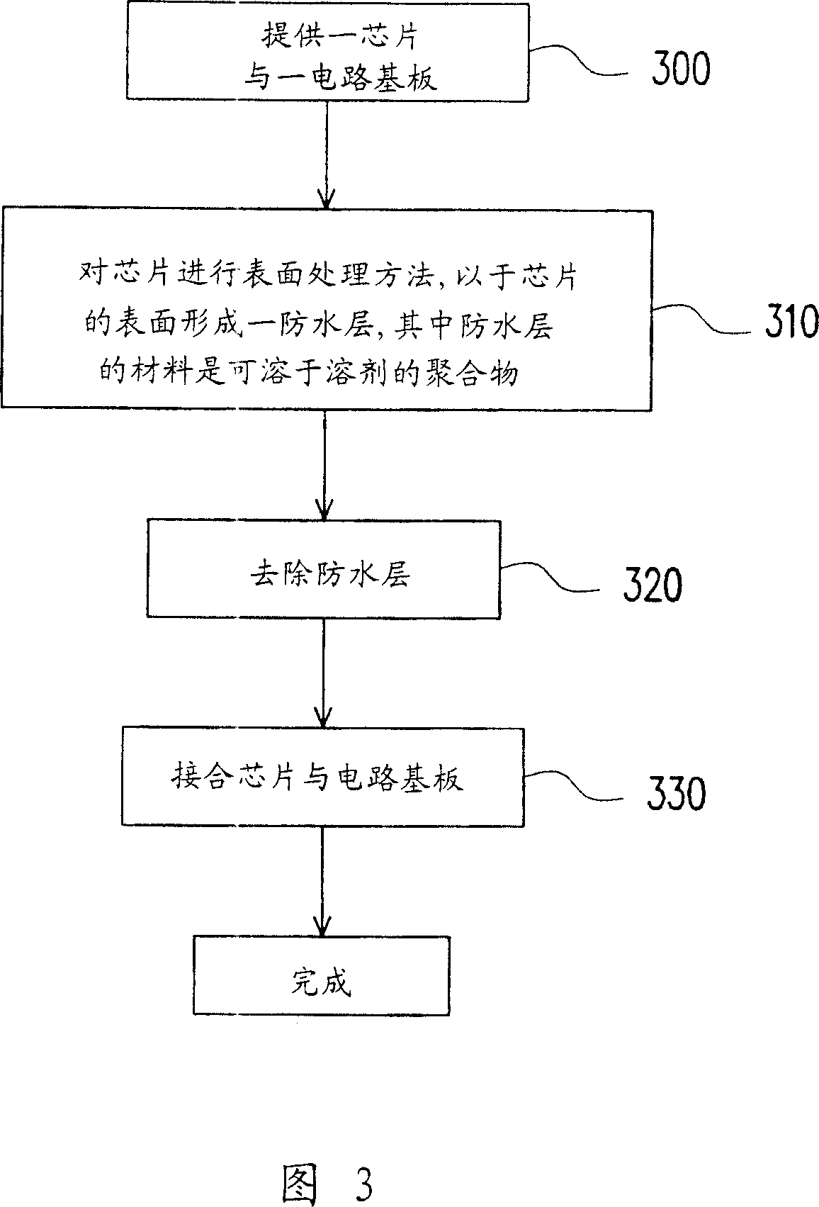
[0035] Please refer to FIG. 1A first. The present invention proposes a surface treatment method for microelectronic components, which is suitable for a chip 10 that has completed the back-end process (BEOL), wherein the chip 10 is, for example, composed of a substrate 100, several layers of dielectric layers 102, 104 and 110 , the plug 106 and the pad 108 are formed. The solder pads 108 and the outermost dielectric layer 110 are exposed on the surface of the chip 10 . The above structure of the chip 10 is just an example, and is not intended to limit the scope of application of the present invention.

[0036] Next, please refer to FIG. 1B , the method of this embodiment is to form a layer of solvent-soluble polymer layer (solvent dissolvable polymer layer) 120 on the surface of the chip 10, and its thickness is, for ...


PUM


Abstract

A storage structure for a micro-electronic component is provided, which comprises a chip with completed back end technique and a polymer layer that is covered on the surface of the chip and can be dissolved in solvent. Because the polymer layer is able to isolate the surface and external environment of the chip, the invention is able to prevent the occurrence of erosion, fading or stratification on the surface of the chip.

Description

technical field [0001] The present invention relates to a treatment for microelectronic devices, in particular to a surface treatment, sorting and assembling method of microelectronic devices and a storage structure thereof. Background technique [0002] Microelectronic components are often affected by the external environment during storage prior to final assembly. For example, after a long period of storage of microelectronic components, it is found that the surface of the chip (chip) of the microelectronic components will be corroded (corrosion), discolored (discolor) or delaminated (delaminating), which will lead to the deterioration of the final product. crumbs. Contents of the invention [0003] The purpose of the present invention is to provide a surface treatment method for microelectronic components to protect the chip surface of the microelectronic components from adverse external environment without complex and high-cost processes. [0004] Another object of t...

Claims


Application Information

Patent Timeline
Patent Type & Authority Applications(China)
IPC IPC(8): H01L21/00H01L21/66H01L21/50
Inventor 张光晔于劲
Owner UNITED MICROELECTRONICS CORP
Why Eureka
Try Eureka